Carbon nanotube for electron emitting source, and method for mfg. same
An electron emission source and carbon nanotube technology, which is applied in the direction of carbon nanotubes, nanotechnology for information processing, nanostructure manufacturing, etc., can solve the problems of expensive power circuits and increased costs
- Summary
- Abstract
- Description
- Claims
- Application Information
AI Technical Summary
Problems solved by technology
Method used
Image

Examples
no. 1 approach
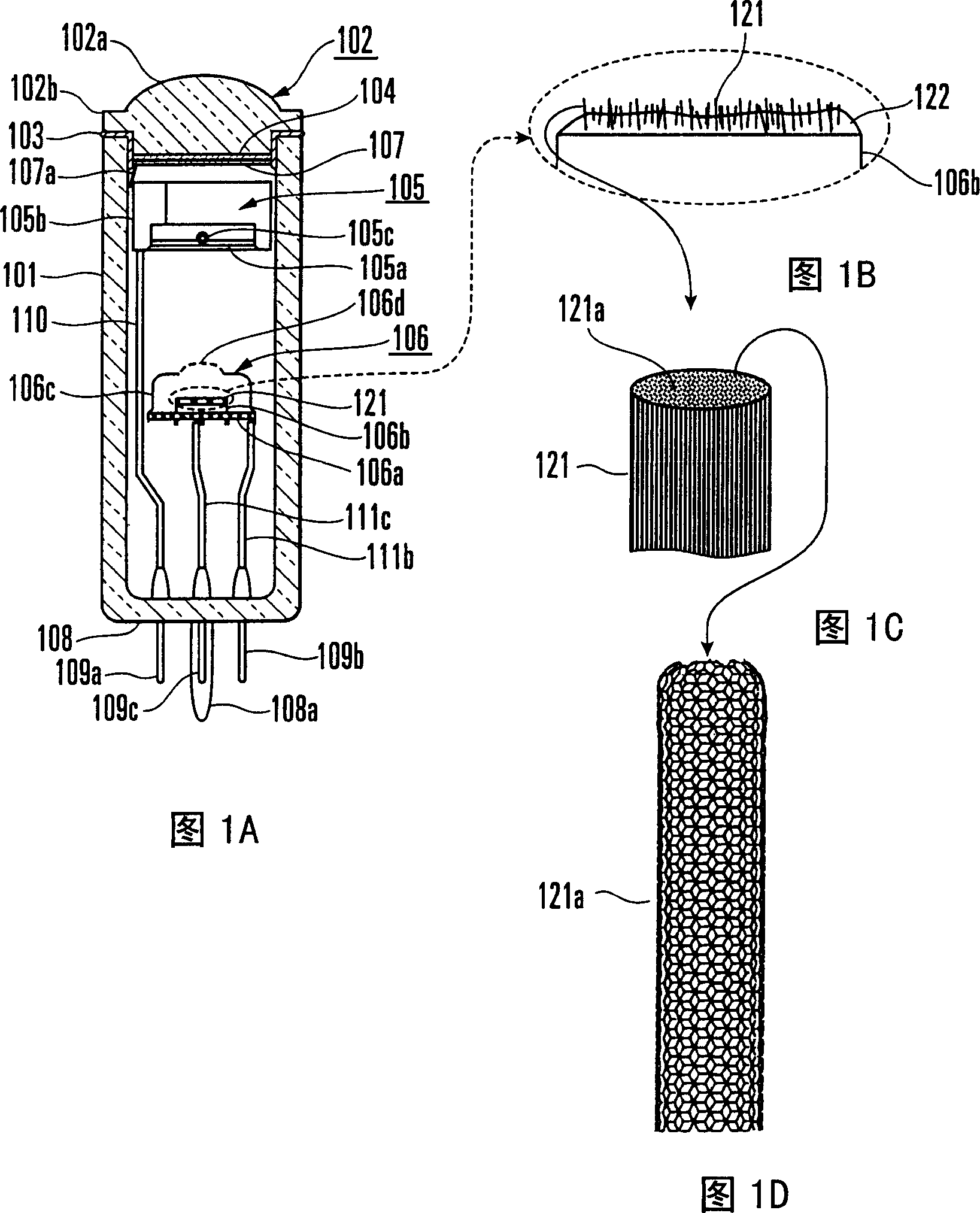
[0039] 1A-1E show the arrangement of a vacuum fluorescent display (picture tube) using an electron emission source according to one embodiment of the present invention.
[0040] The picture tube is designed such that a face glass 102 is bonded / fixed to a cylindrical glass bulb 101 with low-melting frit glass 103 to form a vacuum vessel (envelope). In the vacuum vessel, a phosphor screen 104, an anode electrode assembly 105, and a cathode assembly 106 serving as an electron emission source are arranged.
[0041]Note that in the process of manufacturing this picture tube, after the anode electrode assembly 105 and the cathode assembly 106 are arranged in the glass bulb 101, the face glass 102 on which the phosphor mesh 104 is formed is bonded / fixed to the glass bulb 101 superior.
[0042] A spherical portion 102 a of a convex lens is formed on the front surface of the face glass 102 , and a collar-shaped step portion 102 b is formed on the edge of the face glass 102 . The phos...
no. 2 approach
[0069] The following reference Figure 2A , 2B, and 3 describe an electron emission source according to a second embodiment of the present invention.
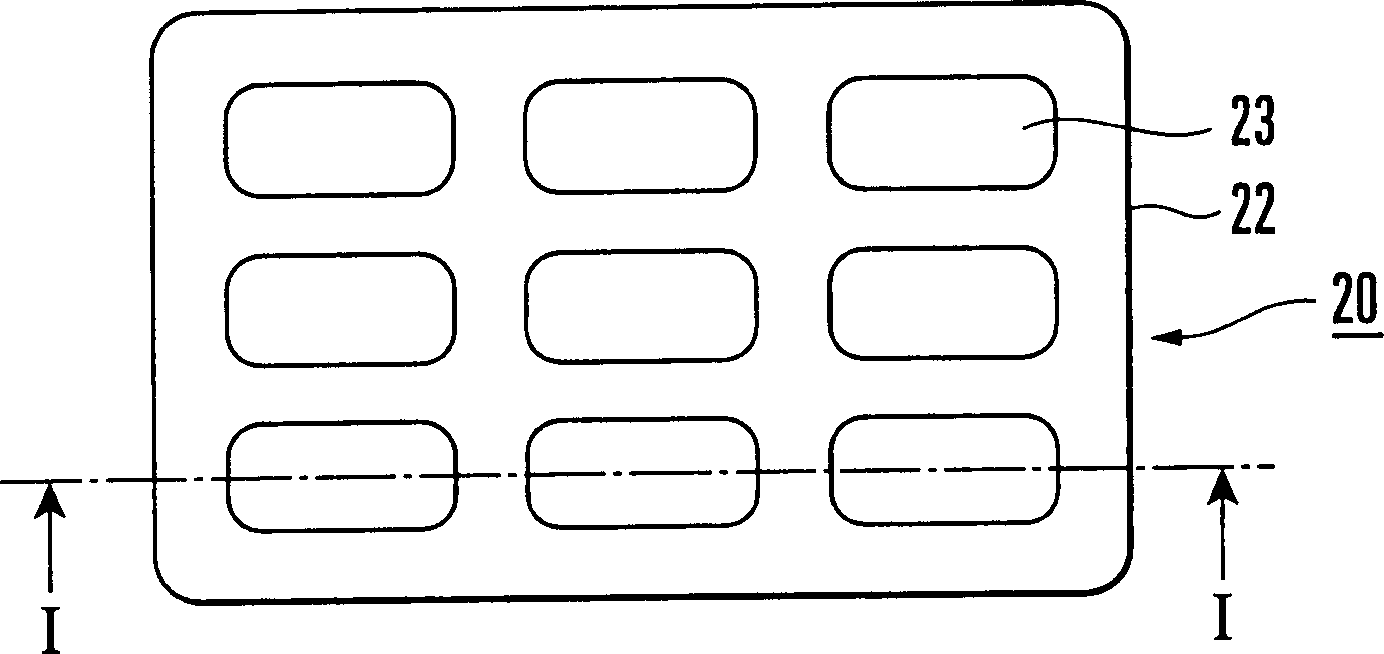
[0070] Figure 2A with 2B The arrangement of the electron emission source according to this embodiment is shown. Such as Figure 2A with 2B As shown, the electron emission source 20 is designed such that carbon nanotubes are arranged on the surface of a substrate 21 having many perforations 23 and perforation walls 24 .
[0071] The substrate 21 is made of a material used as a catalyst to generate CNTs, such as pure iron or an alloy containing iron. In this case, the substrate 21 has a thickness of 0.05-0.20 mm, and has perforations 23 each having a width of 0.05-0.2 mm, arranged in a matrix form, thus having a lattice-like shape.
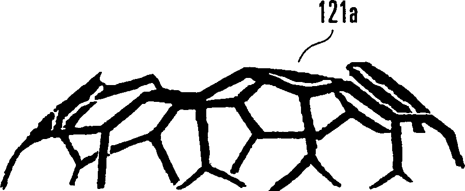
[0072]While being curled or entangled, CNTs respectively having a thickness of about 0.6-100 nm and a length of about 1 μm or more to less than 100 μm are almost uniformly formed on the surfac...
no. 3 approach
[0089] The following reference Figure 4 and 5 , describes an electron emission source according to a third embodiment of the present invention. Note that the same reference numerals as those of the second embodiment denote the same components of the electron emission source in the third embodiment, and a detailed description thereof is omitted.
[0090] In the electron emission source according to this embodiment, CNTs extend vertically from the surface of the matrix-shaped substrate 21 and the perforated walls 24 having the same shapes as those of the electron emission source according to the second embodiment. That is, in this embodiment, the CNTs forming the coating layer 22 extend vertically without curling. Note that, taking the metal part of the lattice as an example, "vertically extending" means that the CNTs extend upward from the upper surface of the metal part, downward from the lower surface, and laterally from the side surfaces.
[0091] Figure 4 An electron ...
PUM
| Property | Measurement | Unit |
|---|---|---|
| thickness | aaaaa | aaaaa |
| length | aaaaa | aaaaa |
| width | aaaaa | aaaaa |
Abstract
Description
Claims
Application Information