Display device, electronic apparatus and method for mfg. display device

A technology of a display device and a manufacturing method, which is applied in the manufacture of discharge tubes/lamps, electrode systems, and semiconductor/solid-state devices, etc., can solve the problems of small luminous quantity and large luminous quantity, and can suppress the shift of luminous intensity. Effect

Inactive Publication Date: 2003-07-02
ELEMENT CAPITAL COMMERCIAL CO PTE LTD
View PDF0 Cites 9 Cited by
  • Summary
  • Abstract
  • Description
  • Claims
  • Application Information

AI Technical Summary

Problems solved by technology

Since the amount of light emitted from the light emitting layer 910b is proportional to the number of injected holes, there is a problem that a portion with a large amount of light emitted and a portion with a small amount of light emitted are generated in one light emitting layer.

Method used


Image

  • Display device, electronic apparatus and method for mfg. display device
  • Display device, electronic apparatus and method for mfg. display device
  • Display device, electronic apparatus and method for mfg. display device

Examples


Embodiment 1

[0087] Next, Embodiment 1 of the present invention will be described with reference to the drawings.

[0088] figure 1 A schematic top view showing the wiring structure of the display device of this embodiment, figure 2 A schematic plan view and a schematic cross-sectional view of the display device of this embodiment are shown.

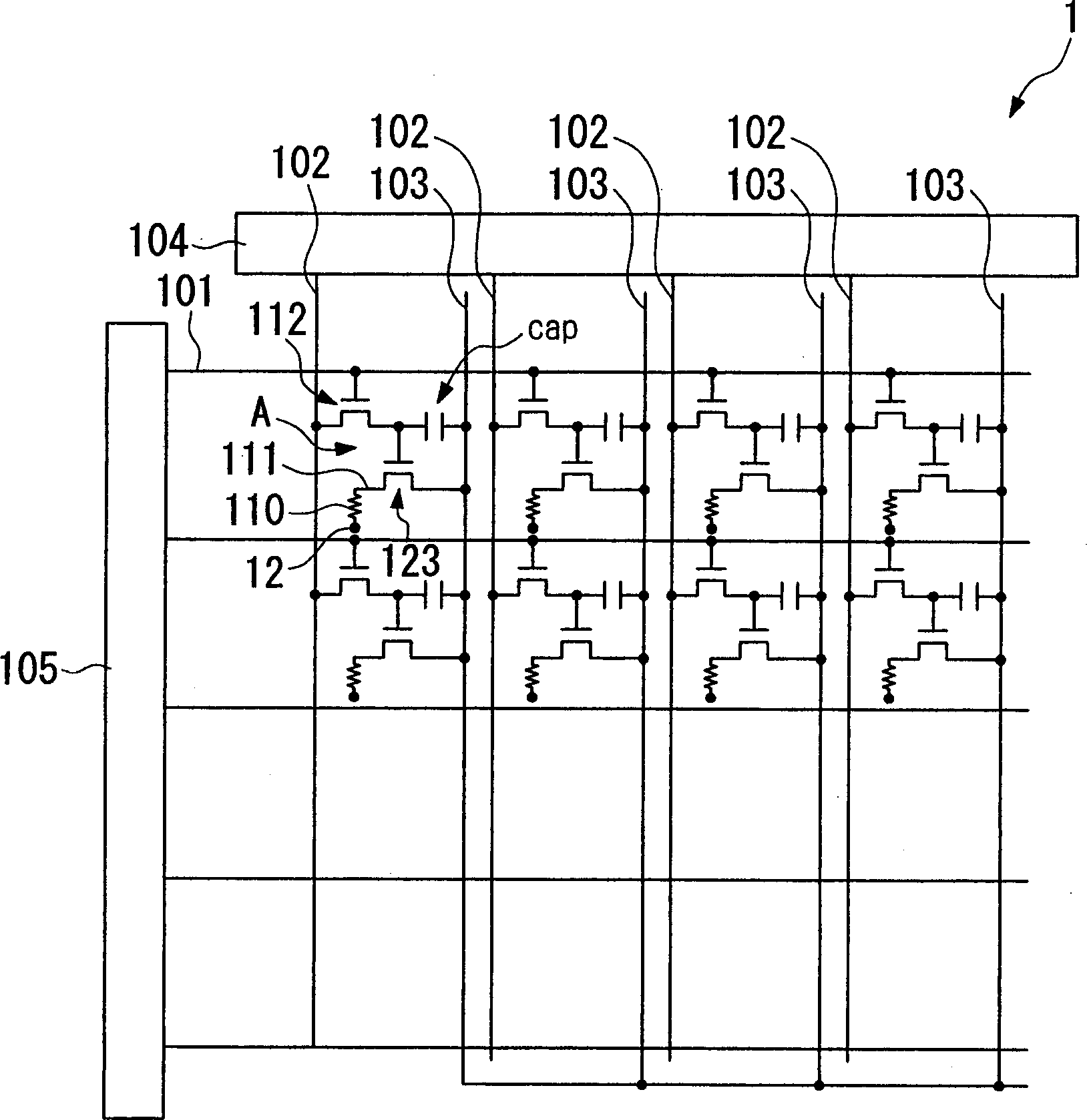
[0089] Such as figure 1 As shown, the display device 1 of this embodiment has a structure in which a plurality of scanning lines 101, a plurality of signal lines 102 extending in a direction intersecting the scanning lines 101, and a plurality of power supply lines 103 extending in parallel are respectively provided, and each A pixel region A is provided near each intersection of the scanning line 101 and the signal line 102 .

[0090] On the signal line 102, a data-side driver circuit 104 having a shift register, a level shifter, a video line, and an analog switch is connected. Also, a scanning line-side driver circuit 105 having a shift regi...

Embodiment 2

[0274] Next, Embodiment 2 of the present invention will be described with reference to the drawings. It should be noted that in the following description, the same reference numerals are used for the same parts as in the first embodiment, and part of the description thereof is omitted.

[0275] Figure 21 It is a sectional view showing the display device of the second embodiment.

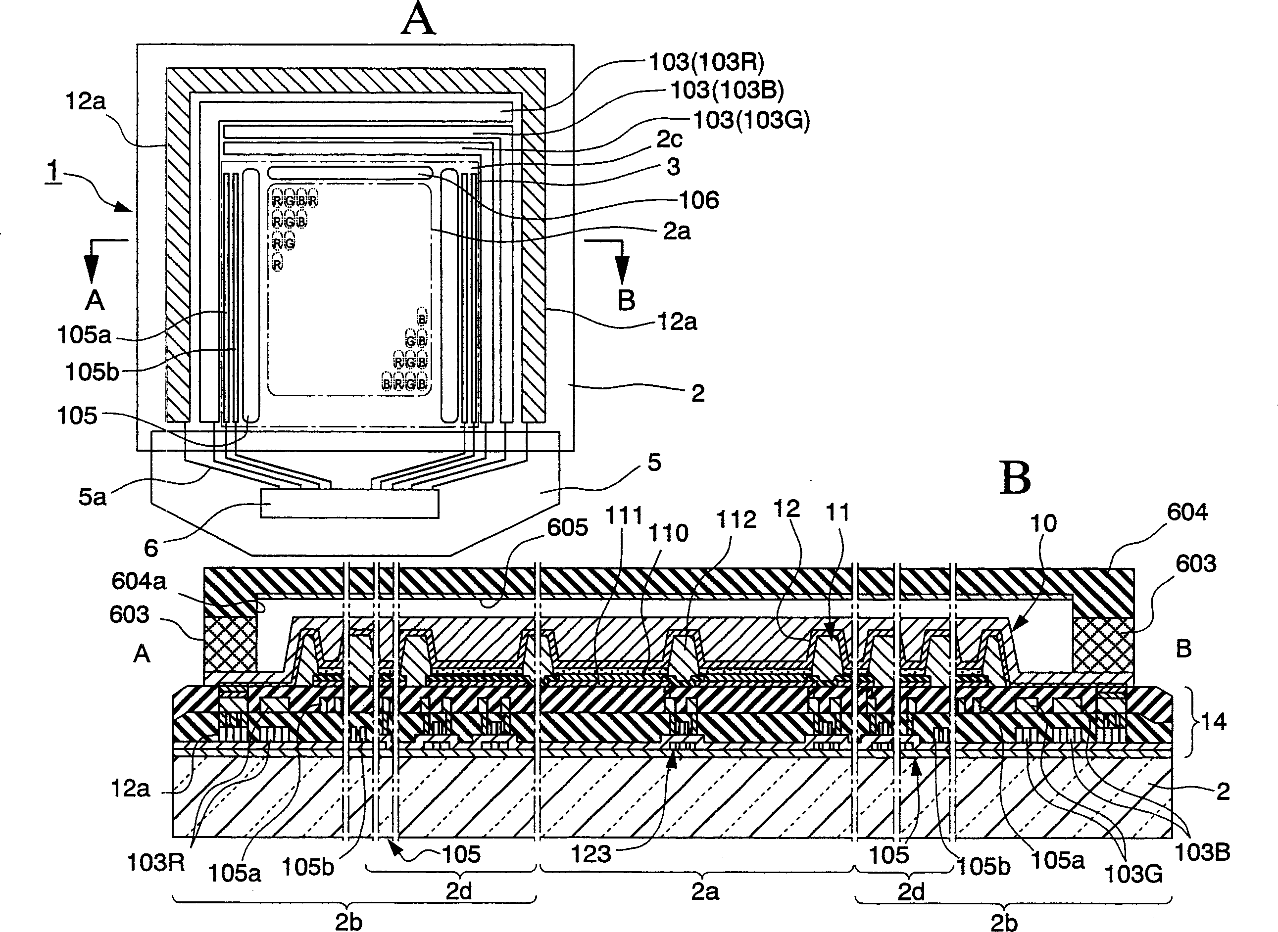
[0276] Such as Figure 21 As shown, the display device of this embodiment includes: a substrate 2', a light emitting element part 11 having light emitting elements arranged in a matrix and formed on the substrate 2', and a cathode 12' formed on the light emitting element part 11' . The display element 10' is constituted by the light emitting element portion 11 and the cathode 12'.

[0277] The display device of this embodiment has a so-called top-emission type structure in which the side of the sealing portion 3' is used as the display surface. As the substrate 2', a transparent substrate (or a ...

Embodiment 3

[0309] Next, a specific example of the display device including Embodiment 1 or 2 will be described.

[0310] Figure 23 A is a perspective view showing an example of a mobile phone. exist Figure 23 In A, reference numeral 600 denotes a mobile phone body, and reference numeral 601 denotes a display unit using the display device.

[0311] Figure 23 B is a perspective view showing an example of a portable information processing device such as a word processor or a personal computer. exist Figure 23 In B, symbol 700 denotes a signal processing device, symbol 701 denotes an input unit such as a keyboard, symbol 703 denotes a main body of an information processing device, and symbol 702 denotes a display unit using the above-mentioned display device.

[0312] Figure 23 C is an example representing a watch-type electronic instrument. exist Figure 23 In C, reference numeral 800 denotes a watch main body, and reference numeral 801 denotes a display unit using the above-me...


PUM

PropertyMeasurementUnit
thicknessaaaaaaaaaa
thicknessaaaaaaaaaa
thicknessaaaaaaaaaa

Abstract

The present invention provides a display apparatus in which there is no shorting between the electrodes and cathode, and there is little variation in the amount of emitted light within a single luminescent layer. A display apparatus is employed in which first and second bank layers are extended to the peripheral edge section of electrodes, the first bank layer is extended farther towards the center of electrodes than the second bank layer, a first laminated section is formed on the first bank layer, an opening is provided in the bank sections, functional layers are composed of a positive hole injection / transport layer and a luminescent layer, and the positive hole injection / transport layer is composed of a flat section formed on the electrodes and a peripheral edge section formed on the first laminated section of the first bank layer.

Description

technical field [0001] The present invention relates to a display device and a manufacturing method of an electronic instrument and the display device. Background technique [0002] In recent years, light-emitting materials such as organic fluorescent materials have been made into inks, and according to the inkjet method of ejecting the ink (composition) on the base material, a method of patterning the light-emitting materials has been adopted, and sandwiching between the anode and the cathode has been carried out. Development of a color display device having a structure of a light-emitting layer composed of the light-emitting material, particularly an organic EL (Electroluminescence) display device using an organic light-emitting material as a light-emitting material. [0003] Here, a conventional display device (organic EL display device) will be described with reference to the drawings. [0004] Figure 27 It is a schematic cross-sectional view showing a main part of a c...

Claims


Application Information

Patent Timeline
Patent Type & Authority Applications(China)
IPC IPC(8): H05B33/22H01L27/32H01L51/00H01L51/30H01L51/40H01L51/50H05B33/10H05B33/12
CPCH01L27/3246H01L27/3211H01L51/0004H01L51/0036H01L51/0037H01L51/0039H01L51/0043H01L51/0053H01L51/56H10K59/35H10K59/122H10K71/13H10K85/115H10K85/1135H10K85/151H10K85/621H10K85/113H10K71/00H05B33/10
Inventor 关俊一
Owner ELEMENT CAPITAL COMMERCIAL CO PTE LTD
Why Eureka
Try Eureka