Process for preparing strip type array carbon nano tube
A carbon nanotube and strip technology is applied in the field of preparation of strip-type array carbon nanotubes and achieves the effects of low cost, high resolution and uniform structure
- Summary
- Abstract
- Description
- Claims
- Application Information
AI Technical Summary
Problems solved by technology
Method used
Image
Examples
Embodiment 1
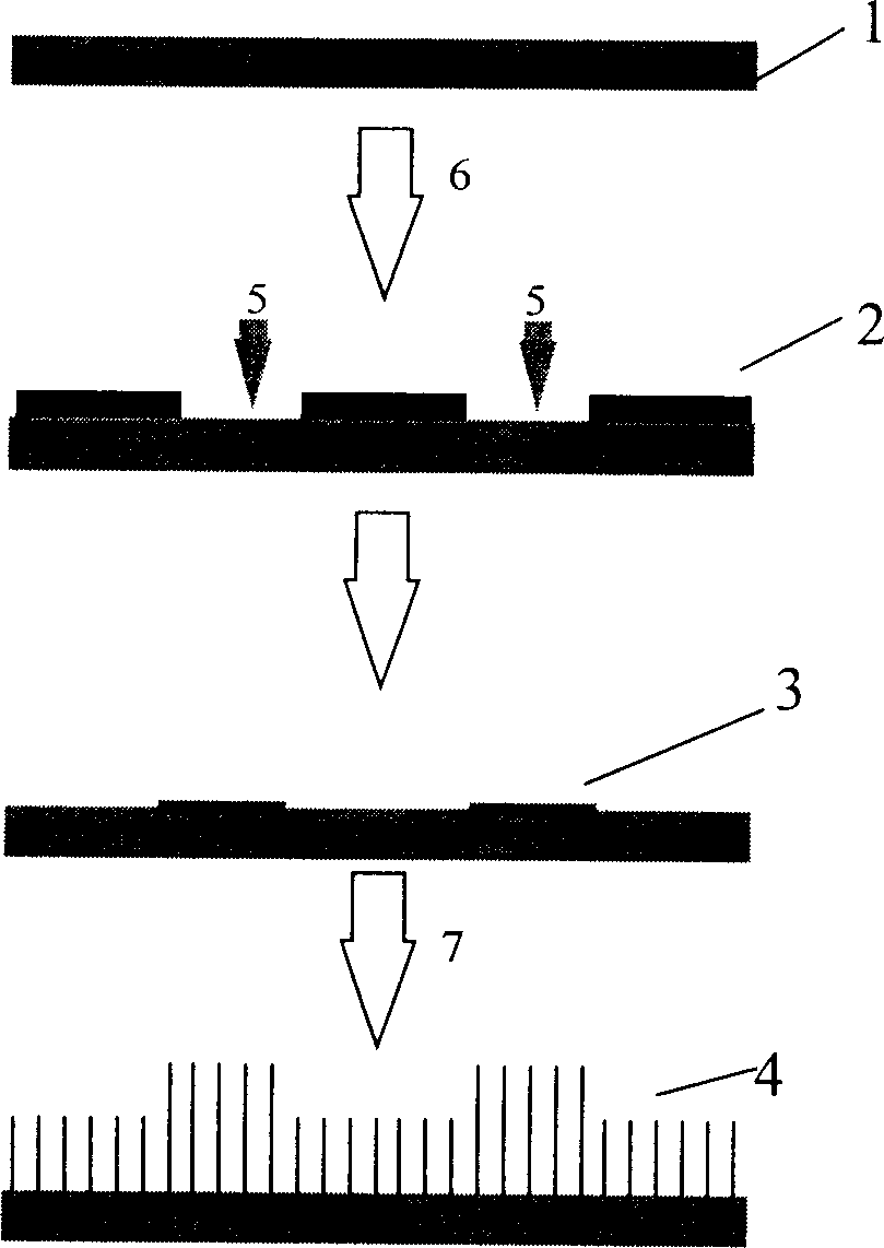
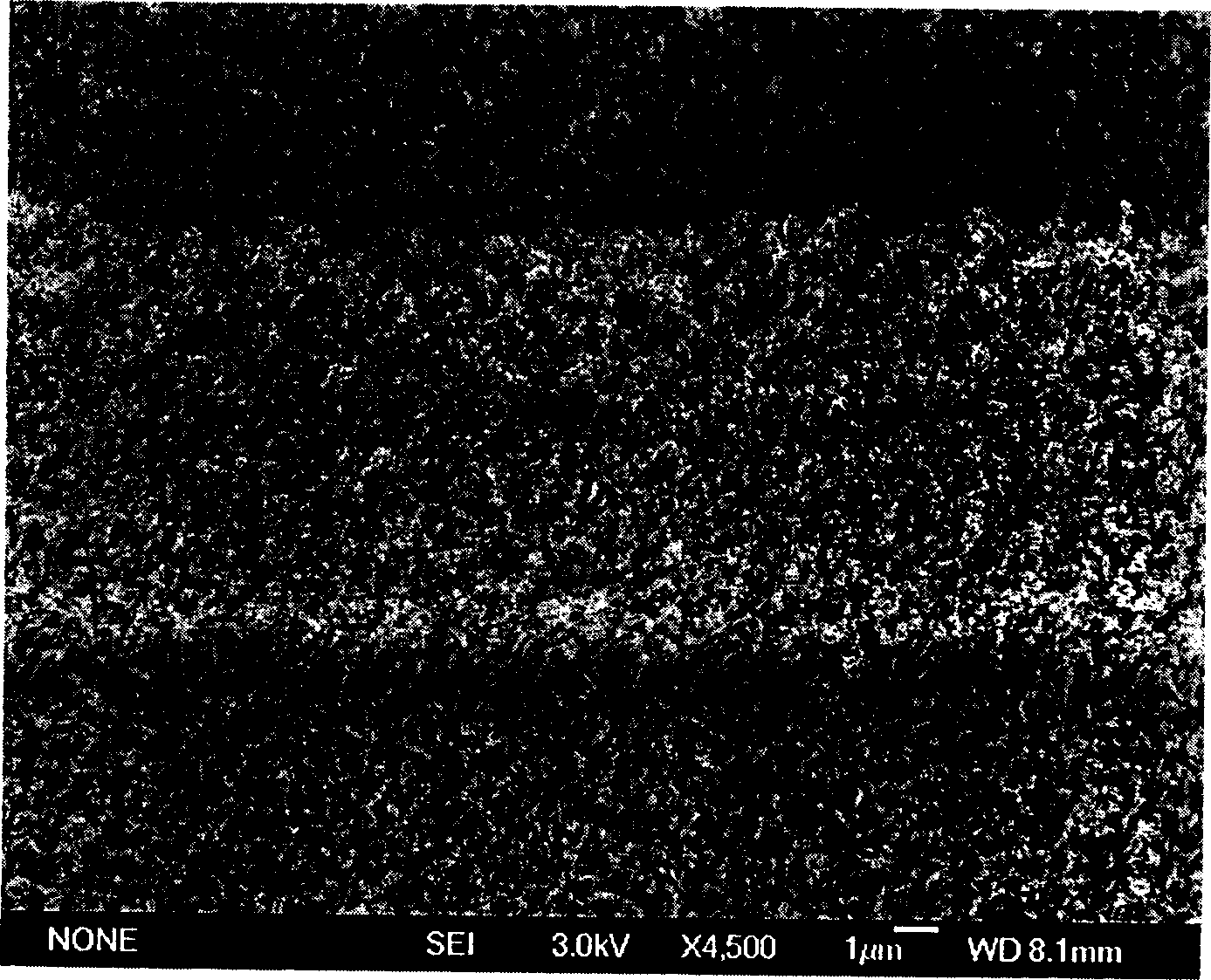
[0023] Embodiment 1 With a width of 18.6 micron strip pattern mask, on a clean quartz glass substrate (1 * 2 cm), vacuum (pressure is 10 -3 Pascal) vapor-deposited a metal aluminum film with a thickness of 250 nm (such as figure 1 shown), the quartz sheet with a striped aluminum film pattern was bombarded with plasma in ammonia gas for 10 minutes, and then put into a reactor consisting of a quartz tube and a tube electric furnace, at a rate of 40 ml per minute Flow into the mixed gas of equal volume of hydrogen and argon, then raise the temperature of the electric furnace to 950 ° C, after constant temperature, add 0.5 g of iron phthalocyanine, crack at high temperature for 5 minutes, close the electric furnace, continue ventilation to make it cool to room temperature (20 ℃), take out the quartz plate, and observe it under a scanning electron microscope, you can get the following figure 2 In the three-dimensional carbon nanotube array in strip-like structure shown, the strip...
Embodiment 2
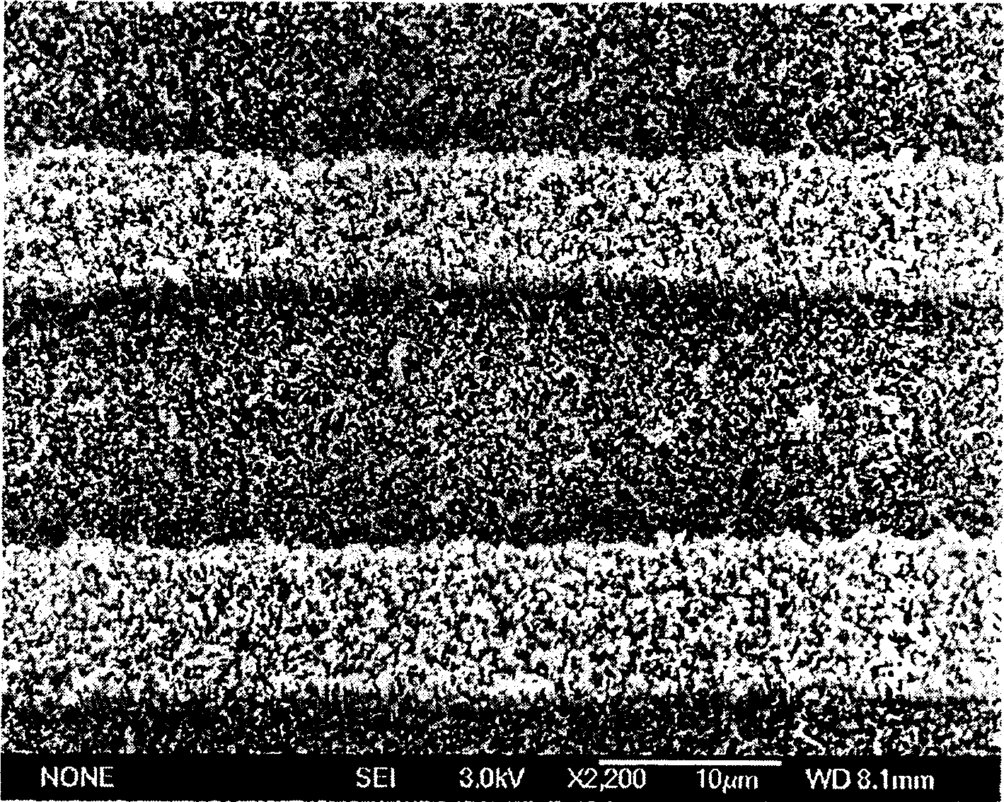
[0024] Example 2 According to the preparation method of Example 1, except that the strip width of the mask was reduced to 8.5 and 6.5 microns, two three-dimensional carbon nanotube arrays with a striped structure of 8.5 and 6.5 microns in width were prepared. The carbon nanotubes inside the band region are 1.4 microns longer than those outside the region. (Such as image 3 shown)
Embodiment 3
[0025] Example 3 According to the preparation method of Example 1, only the strip widths of the mask are changed to 3.0, 2.0, 9.3, 1.3, and 1.0 microns respectively, and the obtained widths are 3.0, 2.0, 9.3, 1.3, and 1.0 microns. A three-dimensional carbon nanotube array in a strip-like structure, and the carbon nanotubes in the strip region are 1.4 microns longer than those outside the region. (Such as Figure 4 shown)
PUM
| Property | Measurement | Unit |
|---|---|---|
| thickness | aaaaa | aaaaa |
| diameter | aaaaa | aaaaa |
| length | aaaaa | aaaaa |
Abstract
Description
Claims
Application Information


