Semiconductor storage device and its making method

A technology of a storage device and a manufacturing method, which is applied in the manufacturing of semiconductor/solid-state devices, semiconductor devices, transistors, etc., can solve the problems of increasing the number of guaranteed rewrites, reducing the characteristics, and difficulty, and achieving the effect of improving the data retention characteristics.

Inactive Publication Date: 2003-10-15
KK TOSHIBA
View PDF0 Cites 1 Cited by
  • Summary
  • Abstract
  • Description
  • Claims
  • Application Information

AI Technical Summary

Problems solved by technology

[0015] In the conventional memory element manufactured as above, the characteristic degradation in the repeated test of data rewriting is remarkable.
In particular, in the high-temperature storage test (data retention test) performed after the repeated rewrite test, the defect that "0" data (the state of accumulating negative charge on the floating gate electrode) becomes "1" data occurs, and the guaranteed number of rewrites is increased. become difficult

Method used


Image

  • Semiconductor storage device and its making method
  • Semiconductor storage device and its making method
  • Semiconductor storage device and its making method

Examples


Embodiment approach 1

[0048] In Embodiment 1, Al is used as a layer for trapping hydrogen or a layer for suppressing hydrogen diffusion 2 o 3 (aluminum oxide) film, the Al is formed on the upper layer of the memory element 2 o 3 membrane.

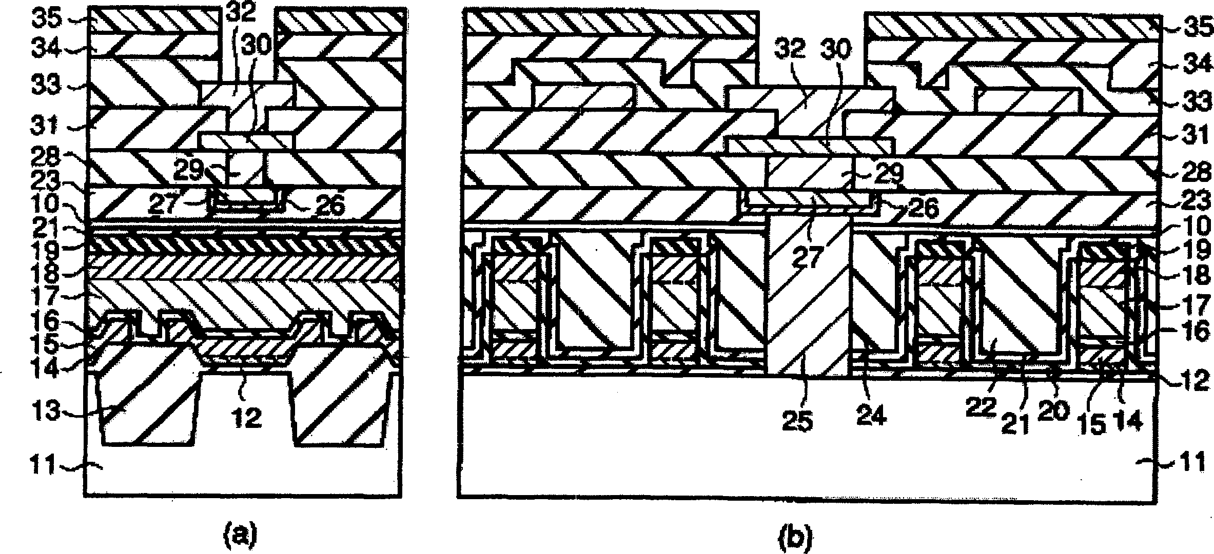
[0049] exist figure 1 In (a), a cross-sectional view of the nonvolatile semiconductor memory device according to Embodiment 1 of the present invention is shown. figure 1 (b) show relative figure 1 (a) Cross-sectional view of the nonvolatile semiconductor memory device in the vertical direction. Hereinafter, the structure of the nonvolatile semiconductor memory device according to Embodiment 1 will be described.

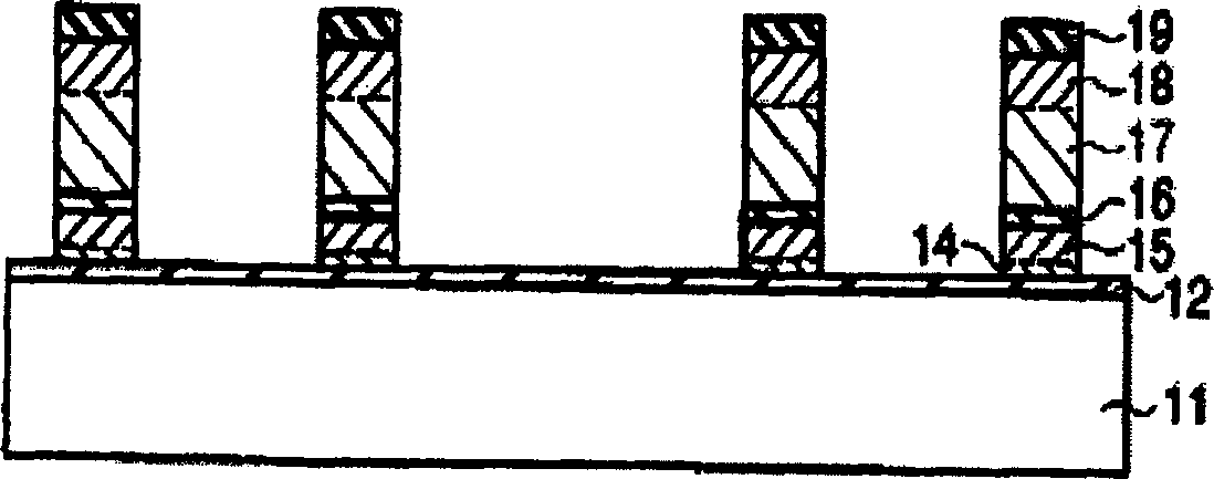
[0050] like figure 1 As shown in (a) and (b), in the nonvolatile semiconductor memory device according to Embodiment 1, Al is formed as a layer that traps hydrogen or a layer that suppresses hydrogen diffusion on the upper layer of the memory element. 2 o 3 Film 10. Then, the Al 2 o 3 The film 10 is located between the memory element and...

Embodiment approach 2

[0075] Embodiment 2, forming Al 2 o 3 The position of the film is different from Embodiment 1, and the Al 2 o 3 A film is formed on the memory element.

[0076] Figure 8 (a) is a cross-sectional view showing a nonvolatile semiconductor memory device according to Embodiment 2 of the present invention. Figure 8 (b) is to show relative Figure 8 (a) Cross-sectional view of the nonvolatile semiconductor memory device in the vertical direction. Hereinafter, the structure of the nonvolatile semiconductor memory device according to Embodiment 2 will be described.

[0077] like Figure 8 As shown in (a) and (b), in the nonvolatile semiconductor memory device of Embodiment 2, the difference from Embodiment 1 is that Al 2 o 3 The film 10 is formed on the third silicon oxide film 23 . Then, as in Embodiment 1, Al 2 o 3 The film 10 is located between the memory element and the second metal layer 32 . The description of other structures is omitted because they are the same a...

Embodiment approach 3

[0089] Embodiment 3, forming Al 2 o 3 The position of the film is different from Embodiment 1, the Al 2 o 3 The film is formed on the silicon oxide film on the upper wiring.

[0090] Figure 13 (a) is a cross-sectional view showing a nonvolatile semiconductor memory device according to Embodiment 3 of the present invention. Figure 13 (b) is to show relative Figure 13 (a) A cross-sectional view of the nonvolatile semiconductor memory device in the vertical direction. Hereinafter, the structure of the nonvolatile semiconductor memory device according to Embodiment 3 will be described.

[0091] like Figure 13 As shown in (a) and (b), in the nonvolatile semiconductor memory device of Embodiment 3, the difference from Embodiment 1 is that Al 2 o 3 The film 10 is formed on the sixth silicon oxide film 33 on the second metal layer 32 . The description of other structures is omitted because they are the same as those in the first embodiment.

[0092] Figure 14 to Figur...


PUM


Abstract

Provided are a nonvolatile semiconductor memory device capable of improving data retention characteristics and a method of manufacturing the same. On the upper layer of the memory element, there is at least one layer including at least one of the following groups: a silicon oxide film doped with nitrogen; a silicon oxide film doped with Al; an oxide of Al; a silicon oxide film doped with Ti; Nitrogen and two of the three kinds of Al and Ti silicon oxide film; silicon oxide film with nitrogen and three kinds of Al and Ti added; Ti oxide; Ti and Al oxide; made of Ti, Ni, Co , Zr, Cu, Pt, V, Mg, U, Nd, La, Sc metal group consisting of a single metal layer; metals containing two or more of these metal groups account for at least 50% of the whole A layer composed of a binary or higher alloy; a layer composed of a nitride of the alloy; or a layer composed of a hydride of the alloy (such as the Al2O3 film 10).

Description

technical field [0001] The present invention relates to a nonvolatile semiconductor storage device and a manufacturing method thereof, in particular to a flash memory with a floating gate. Background technique [0002] Hereinafter, the prior art and its problems will be described with reference to the drawings. [0003] Figure 18 (a) shows a cross-sectional view of a conventional nonvolatile semiconductor memory device. Figure 18 (b), showing the relative Figure 18 (a) Cross-sectional view of the nonvolatile semiconductor memory device in the vertical direction. like Figure 18 As shown in (a) and (b), in the nonvolatile semiconductor memory device of the prior art, silicon oxide films 123, 128, 131, 133, silicon nitride film 134, polyamide film are stacked on the upper layer of the memory element Imine resin 135. [0004] Here, the memory element includes first and second gate insulating films 112 and 116; a floating gate made of first and second polysilicon films 114 ...

Claims


Application Information

Patent Timeline
Patent Type & Authority Applications(China)
IPC IPC(8): H01L21/8247H01L27/115H01L29/788H01L29/792
CPCH01L27/11521H01L27/115H10B69/00H10B41/30
Inventor 角田弘昭小林英行姬野嘉朗柴克育福原成太
Owner KK TOSHIBA
Why Eureka
Try Eureka