
Patsnap Eureka
For R&D, Patsnap Eureka makes reading and utilizing patents & technical documents easy.
Patsnap Eureka AIR
Designed for self-driven R&D workflows. Generate viable solutions, solve complex R&D challenges, empower your innovation with AI.

Patsnap Eureka Materials
Designed for material experts only. Revolutionize your material R&D, from search, analyze, to developing new materials.

TechResearch
Generate reliable direction feasibility study reports for your R&D in just a few steps.

TechSeek
Discover and master advanced knowledge NOW. Basics, ideas, possibilities, all at once.

TechMind
As an expert in R&D Theories, TechMind can generates customized viable solutions instantly.

TechRisk
Analyze your overall solution with one click, know your potential R&D risks in advance.

TechMonitor
Get weekly tech updates, stay abreast of the latest tech innovations and key insights.
Method for eliminatnig defects on wafer by high energy full ion implantation
An ion implantation, silicon wafer technology, applied in electrical components, semiconductor/solid-state device manufacturing, circuits, etc., can solve the problem of reducing silicon wafer metal impurity defects, reducing part of the impurity depth, reducing component qualification rate and electrical properties quality and other issues
- Summary
- Abstract
- Description
- Claims
- Application Information
AI Technical Summary
Problems solved by technology
Method used
Image

Examples
Embodiment Construction
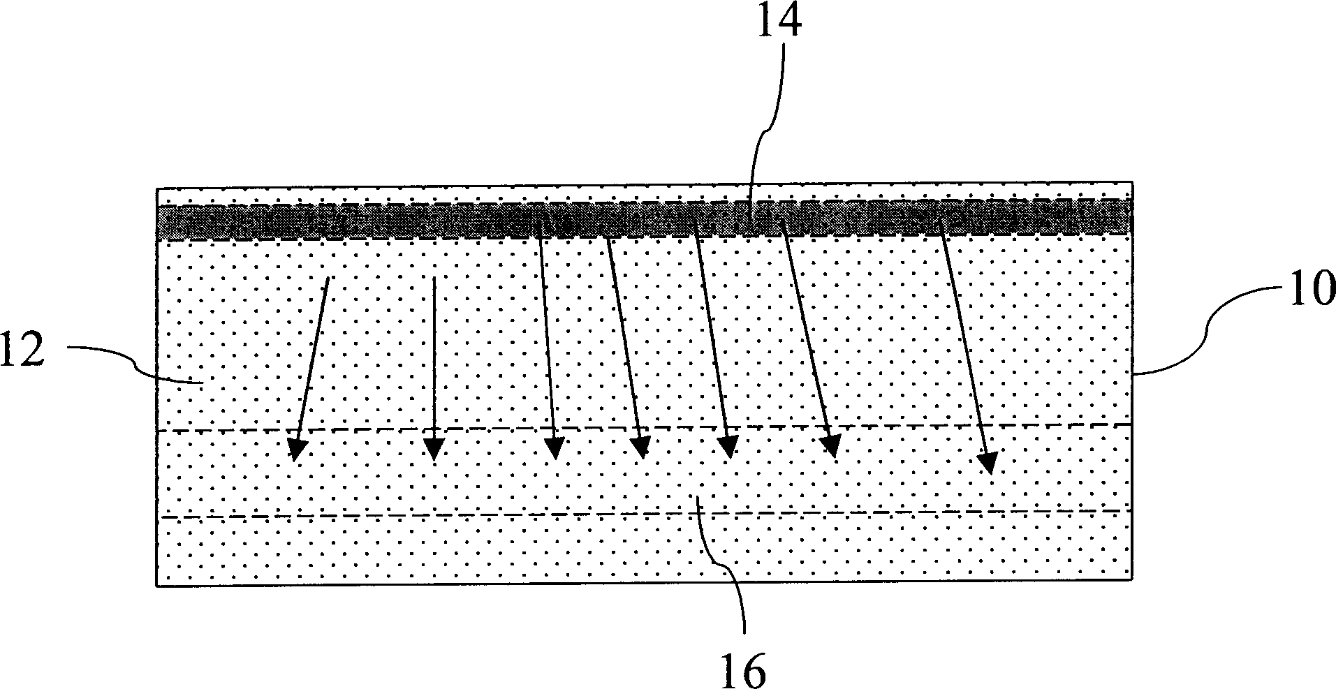
[0014] The present invention uses a high-energy full-scale ion implantation method (VHEBI) to remove impurities and heavy metals on the surface of a silicon wafer that will cause adverse effects on component characteristics, or to remove point defects related to defects, etc., so as to remove defects (gettering) The component formation area on the surface of the silicon wafer is cleaned or free of defects to improve component characteristics and product qualification rate of component manufacturing.
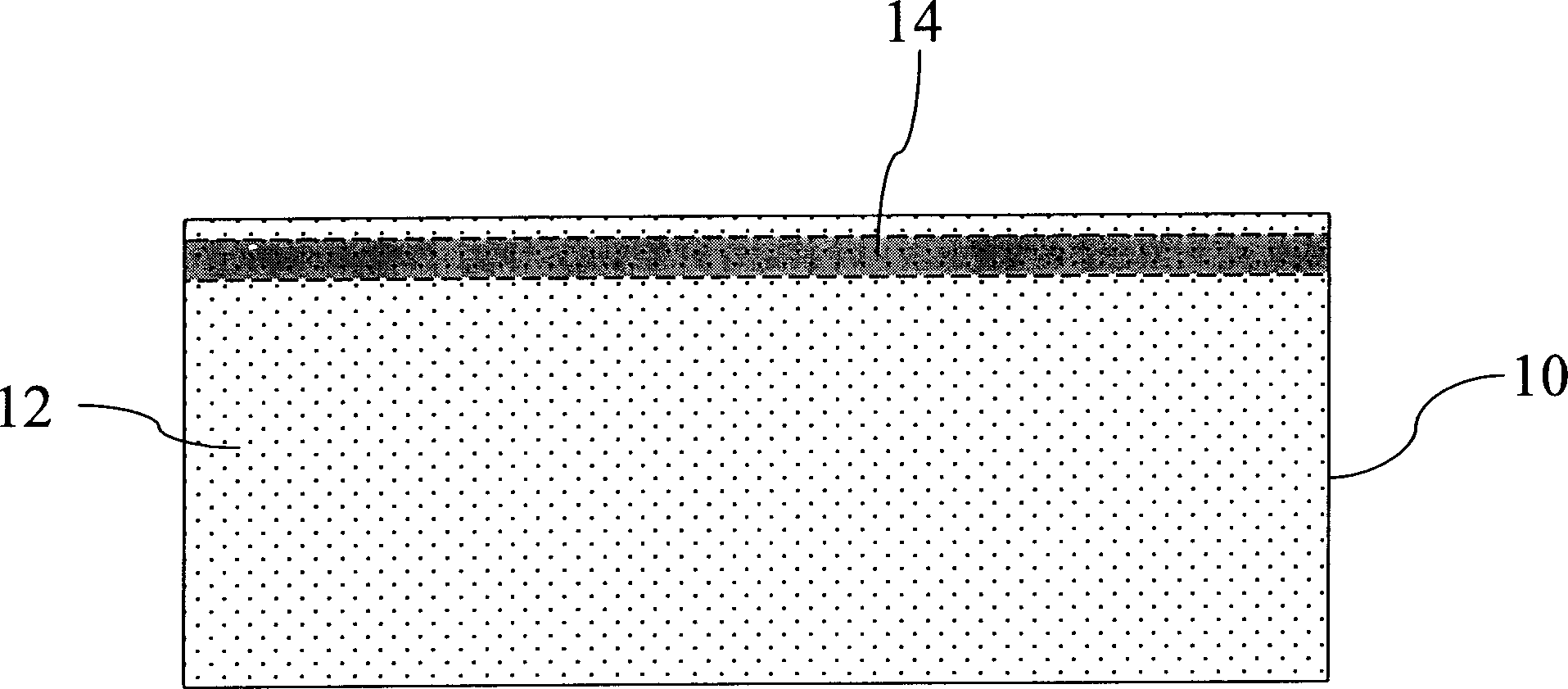
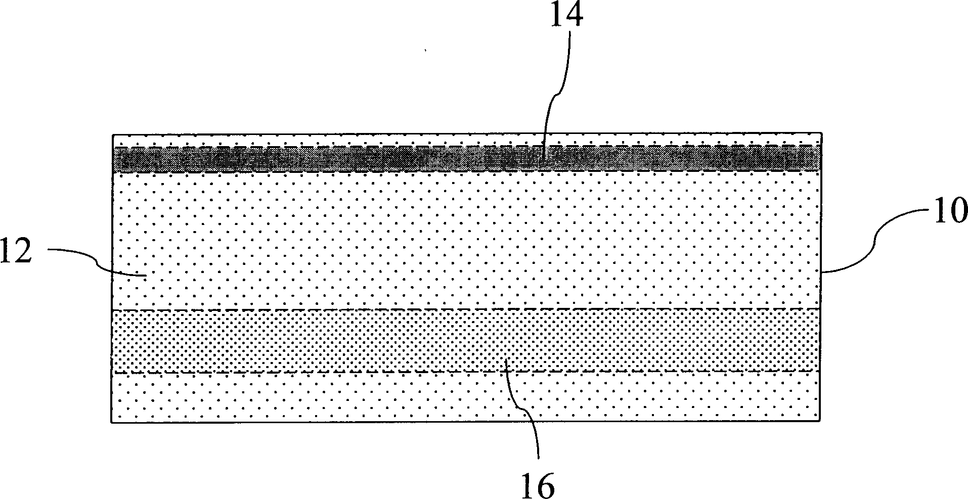
[0015] In the semiconductor wafer forming process, the defects caused by the environmental impurity pollution and thermal stress caused by the growth of single crystal silicon are all left in the silicon wafer 10, and the impurity defects 12 caused by subsequent processing also exist in it, such as figure 1 As shown, especially the impurity defect 12 located in the component forming region 14 on the surface of the silicon wafer 10 often affects the behavior of the carrier (Carrier...
PUM
| Property | Measurement | Unit |
|---|---|---|
| Depth | aaaaa | aaaaa |
Abstract
Description
Claims
Application Information
 - R&D Engineer
- R&D Manager
- IP Professional
- Industry Leading Data Capabilities
- Powerful AI technology
- Patent DNA Extraction
Browse by: Latest US Patents, China's latest patents, Technical Efficacy Thesaurus, Application Domain, Technology Topic, Popular Technical Reports.
© 2024 PatSnap. All rights reserved.Legal|Privacy policy|Modern Slavery Act Transparency Statement|Sitemap|About US| Contact US: help@patsnap.com