Lithographic method of manufacturing device

A device and etching technology, applied in the field of manufacturing devices, can solve the problems of imaging, inability to use lighting devices, etc., to achieve the effect of reducing distance and solving the problem of disabled parameters

Inactive Publication Date: 2004-02-11
KONINKLIJKE PHILIPS ELECTRONICS NV
View PDF9 Cites 12 Cited by
  • Summary
  • Abstract
  • Description
  • Claims
  • Application Information

AI Technical Summary

Problems solved by technology

However, if the mask pattern has a certain (forbidden) symmetry, spatial period (pitch) and/or orientation of the features, then these

Method used


Image

  • Lithographic method of manufacturing device
  • Lithographic method of manufacturing device
  • Lithographic method of manufacturing device

Examples


Embodiment Construction

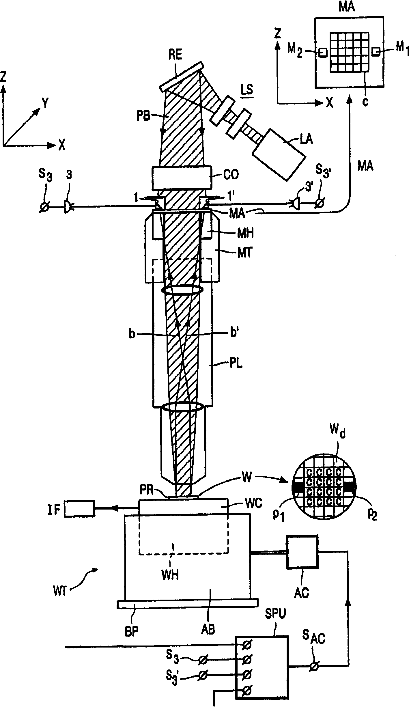
[0116] figure 1 The schematic diagram shows only the most important modules of one embodiment of a lithographic projector. The apparatus comprises a projection column housing a projection device, such as a lenticular projection device PL. On this apparatus is placed a mask holder MH which includes a mask pattern C to be imaged and which is used to transfer a mask MA. The mask holder forms part of the mask table MT. A pedestal WT is disposed in the projection column under the projection lens arrangement. The stage is equipped with a substrate holder WH that supports a substrate W such as a semiconductor substrate (also referred to as a wafer). A photosensitive layer PR such as a photosensitive resin layer is coated on the substrate. The mask pattern C is to be imaged multiple times in the resist layer, each time in another IC region, or stamp Wd. The submount can be moved in the X direction and the Y direction, so after the mask pattern is imaged in one IC region, the next...


PUM


Abstract

For lithographically manufacturing a device with a very high density, a design mask pattern (120) is distributed on a number of sub-patterns (120a, 120b, 120c) by means of a new method. The sub-patterns do not comprise "forbidden" structures (135) and can be transferred by conventional apparatus to a substrate layer to be patterned. For the transfer, a new stack of layers is used, which comprise a pair of a processing layer (22; 26) and an inorganic anti-reflection layer (24; 28) for each sub-pattern. After a first processing layer (26) has been patterned with a first sub-pattern, it is coated with a new resist layer (30) which is exposed with a second sub-pattern, and a second processing layer (22) under the first processing layer is processed with the second sub-pattern.

Description

technical field [0001] The invention relates to a method of manufacturing a device in at least one substrate, the method comprising the steps of: [0002] - generating a design pattern comprising pattern features corresponding to device features to be formed in the layer; [0003] - transferring the design pattern in a resist layer disposed on the base layer; [0004] - removal of material or addition of material from the areas of the layer demarcated by the patterned resist layer; [0005] - sub-patterns respectively comprising different parts of the designed pattern are successively transferred in a corresponding number of resist layers, said resist layers being successively coated on said base layer. [0006] The invention also relates to methods of distributing pattern features of a designed pattern over a number of sub-patterns. [0007] The invention also relates to an assembly of photolithographic submasks which together form a virtual mask for patterning a device wi...

Claims


Application Information

Patent Timeline
IPC IPC(8): G03F7/11G03F1/00G03F7/00G03F7/14G03F7/20G03F7/40H01L21/027H01L21/3213
CPCG03F1/144H01L21/32139G03F1/36G03F7/0035G03F1/26H01L21/027
Inventor P·迪尔克森C·A·H·于费尔曼斯J·范温格尔登
Owner KONINKLIJKE PHILIPS ELECTRONICS NV
Why Eureka
Try Eureka