

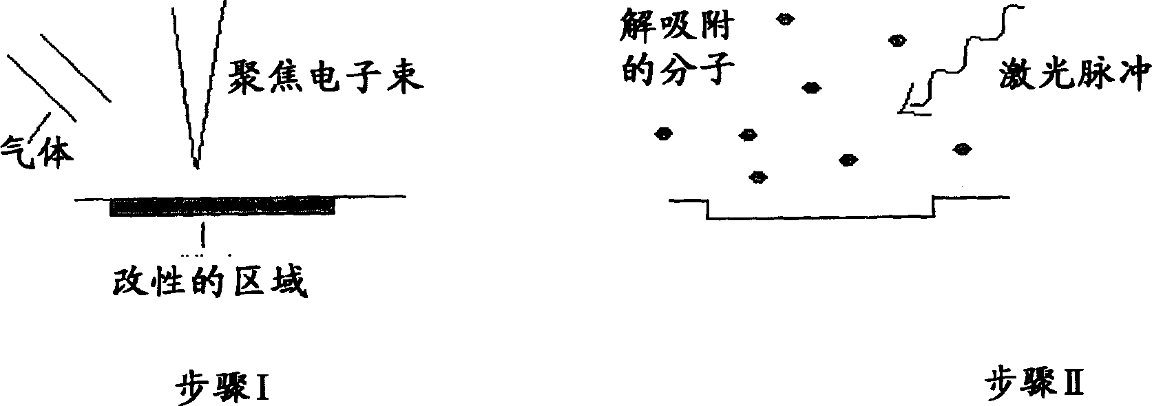
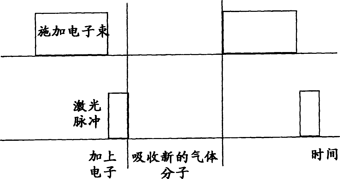
Method for etching surface material with induced chemical reaction by focused electron beam on surface
A technology of focusing electron beams and chemical reactions, which is applied in the processing of photosensitive materials, originals for photomechanical processing, and photoplate-making processes on patterned surfaces, and can solve problems such as opacity, transparency defects, and lack of absorbent materials
- Summary
- Abstract
- Description
- Claims
- Application Information
AI Technical Summary
Problems solved by technology
Method used
Image

Examples
Embodiment Construction
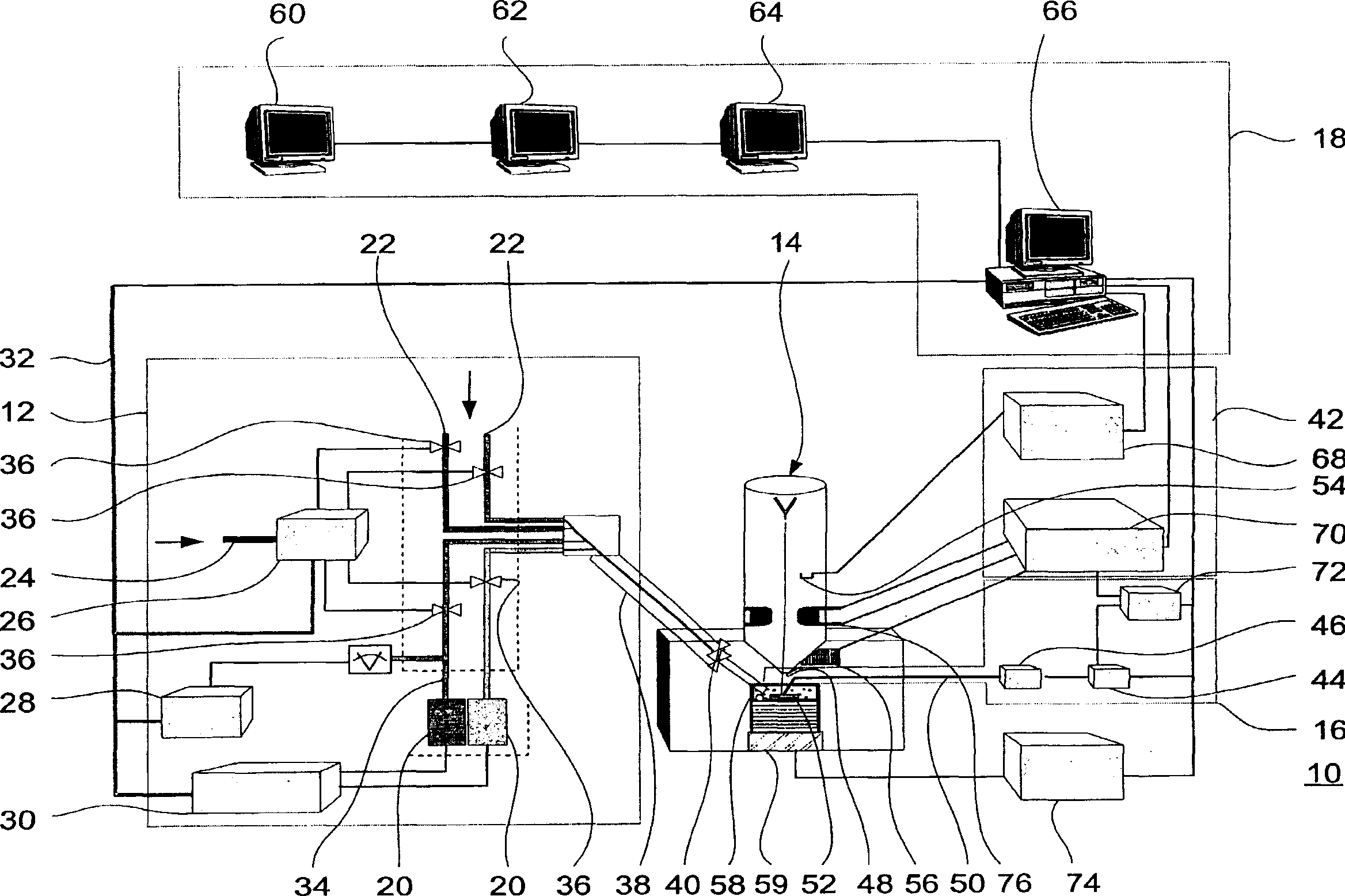
[0045] figure 1 Shown is a schematic assembly diagram of a mask repair system 10 according to the method of the present invention, having a known molecular beam delivery system, hereinafter referred to as gas delivery system 12; a known electron beam system 14; a known photon beam system, hereinafter referred to as the laser beam system 16; and the computer control system 18 for triggering operations in due time and coordinating the beams - molecular beams, photon beams and electron beams.
[0046] The gas supply system 12 comprises a reservoir 20 for liquid or solid precursor - Peltier cooled -; a feed line 22 for a gaseous precursor; a feed line 24 for compressed air; a valve control 26, a pressure gauge 28 and a Temperature control 30 in reservoir 20 . Connection Valve control 26, pressure gauge 28 and temperature gauge are connected to computer control system 18 by means of a CAN open bus.
[0047] The reservoir 20 is connected to a nozzle header 38 by means of a feed pi...
PUM
 Abstract
Description
Claims
Application Information