Semiconductor storage, semiconductor device and semiconductor device control method

A semiconductor and memory technology, which is applied in the field of semiconductor memory and can solve the problems of the memory cell being unable to be located, having large noise, and being unable to provide

Inactive Publication Date: 2004-05-12
HITACHI LTD +1
View PDF1 Cites 9 Cited by
  • Summary
  • Abstract
  • Description
  • Claims
  • Application Information

AI Technical Summary

Problems solved by technology

The open structure has the advantage that the memory cells can be located at all intersections of the data line and the word line and can achieve high integration, but the disadvantage is that it will generate much larger noise in the word line
On the contrary, the advantage of the folded structure is that the noise generated when driving the word line is small, but its disadvantage is that the memory cells cannot be located at all intersections of the data line and the word line, so that it cannot provide high integration

Method used


Image

  • Semiconductor storage, semiconductor device and semiconductor device control method
  • Semiconductor storage, semiconductor device and semiconductor device control method
  • Semiconductor storage, semiconductor device and semiconductor device control method

Examples


no. 1 example

[0086] Specific embodiments of the semiconductor memory element, semiconductor memory, and control method of the present invention are described in detail below with reference to the accompanying drawings. In order to simplify the description, the part of the semiconductor memory will be explained, but in actual operation, these functions are also obtained for the memory combined with contacts and peripheral circuits.

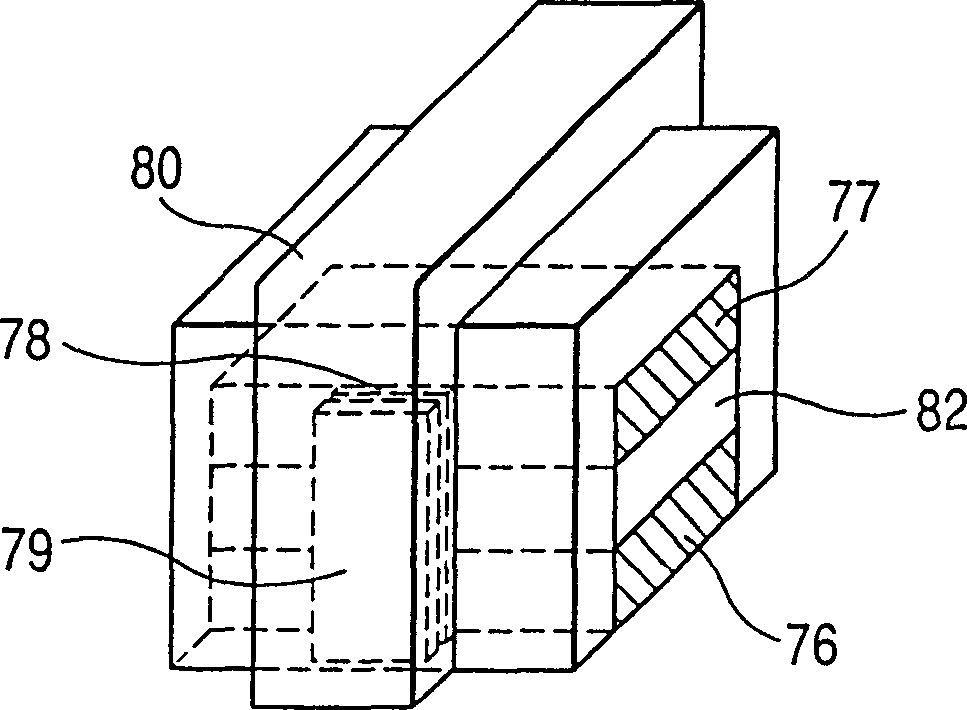
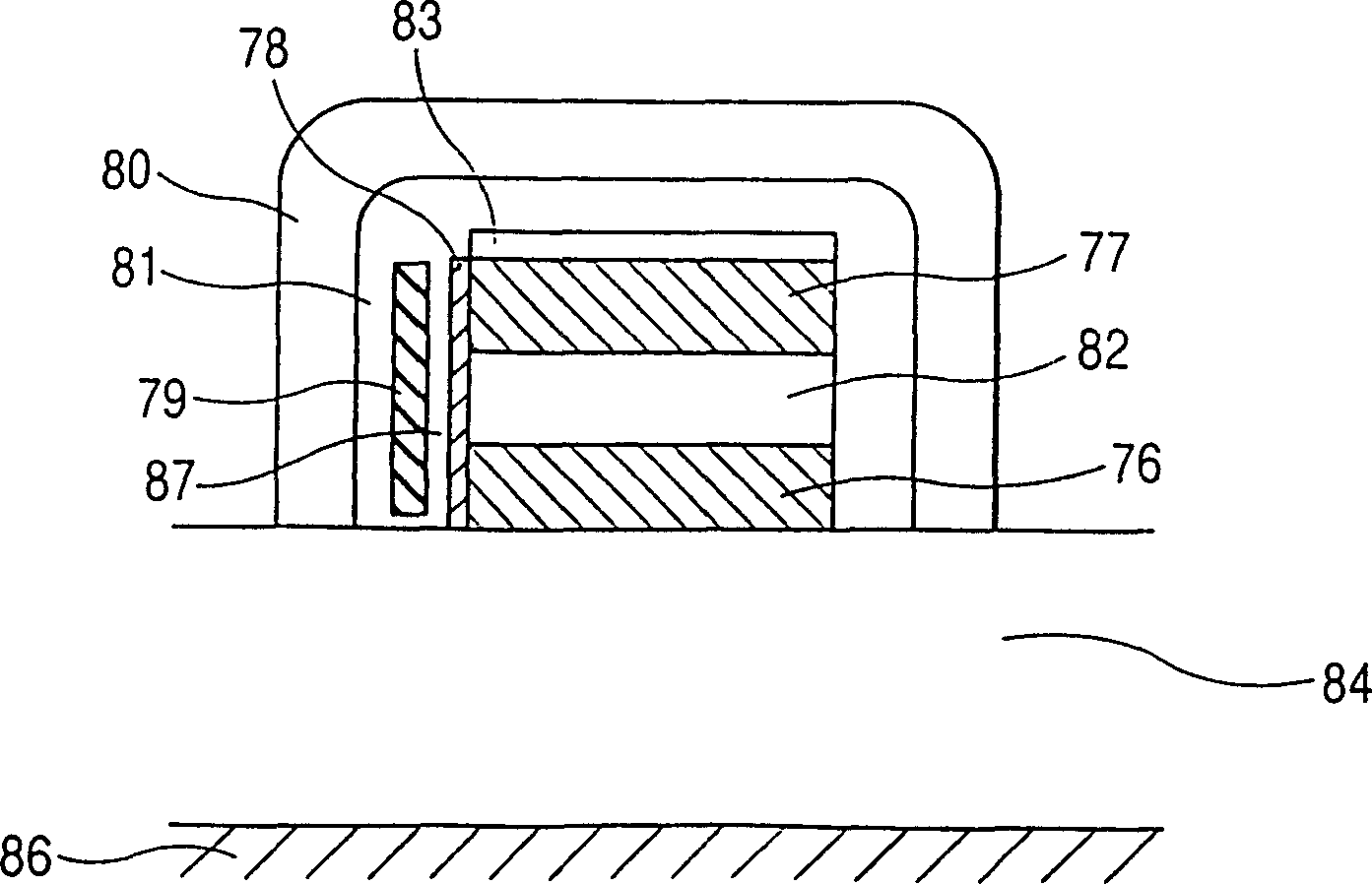
[0087] Figure 1(a) and 1(b) is a structural diagram of the semiconductor memory element of the first embodiment of the present invention. Figure 1(a) is a top slope view. Fig. 1(b) is a cross-sectional view. The source 76 and the drain 77 are regions made of N-type polysilicon with a high impurity concentration. Between the source region 76 and the drain region 77 SiO 2 insulating film 82 . In this SiO 2 On the side surface of the insulating film 82, a channel 78 composed of P-type polysilicon with a thickness of 20 nm and a width of 150 nm is formed. T...

no. 2 example

[0093] Figure 15(a) and 15(b) is a structural diagram of a memory cell according to another embodiment of the present invention. Source 1 and drain 2 are regions made of N-type polysilicon with a high impurity concentration. SiO was fabricated between the source region 1 and the drain region 2 2 insulating film 7. In SiO 2 On the side surface of the insulating film 7 is formed a channel 3 composed of non-doped polysilicon with a width of 20 nm and a thickness of 10 nm. The charge trap region 4 is made of a plurality of polysilicon grains with an average size of 6 nm, and is isolated by an insulating film. Channel 3 and charge trap region 4 via SiO 2 The insulating film 6 is connected to the gate electrode 4 . The distance between the gate electrode and the charge trap region 4 was set at 30 nm. This component is housed in SiO 2 Insulation film 8. Unless there is a special limitation, in the following embodiments, the placement points of the components on the insulat...

no. 3 example

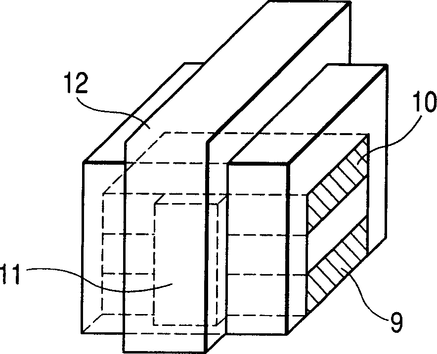
[0096] Figure 2(a) and 2(b)A third embodiment of the invention is shown. This embodiment differs from the second embodiment only in that the channel and the charge trap region 11 are integrated in one unit, and the channel 11 is formed on both sides of the source 9 and the drain 10 . The material of the channel and the charge trap region 11 is a thin non-doped polysilicon layer with an average thickness of about 3nm. In this embodiment, in order to provide a small structure suitable for room temperature work that can be manufactured with a simple process, the potential fluctuations in the polysilicon thin layer with an average thickness of less than 5 nm are used, and the channels and charge trap regions are used in the thin film ( 11) in the natural formation. The crystal grain size in this embodiment is about 3nm, so that the size can be kept within about 10nm even in the lateral direction, and the size of each charge trap region is about the same (10nm).

[0097] One f...


PUM


Abstract

A memory cell with a small surface area is fabricated by forming source lines and data lines above and below and by running the channels to face up and down. The local data lines for each vertically stacked memory cell are connected to a global data line by way of separate selection by a molecular oxide semiconductor, and use of a large surface area is avoided by making joint use of peripheral circuits such as global data lines and sensing amplifiers by performing read and write operations in a timed multiplex manner. Moreover, data lines in multi-layers and memory cells (floating electrode cell) which are non-destructive with respect to readout are utilized to allow placement of memory cells at all intersecting points of word lines and data lines while having a folded data line structure. An improved noise tolerance is attained by establishing a standard threshold voltage for identical dummy cells even in any of the read verify, write verify and erase verify operations. A register to temporarily hold write data in a memory cell during writing is also used as a register to hold a flag showing that writing has ended during write verify. Also, a circuit comprised of one nMOS transistor is utilized as a means to change values on the write-end flag.

Description

[0001] This application is a divisional application of the invention patent application with the application number 99101611.4 and the invention name "semiconductor memory" submitted by Hitachi Manufacturing Co., Ltd. on January 28, 1999. technical field [0002] The present invention relates to a semiconductor memory, a semiconductor device and a control method for the semiconductor device. Background technique [0003] In conventional technology, nonvolatile memories such as flash EEPROMs have been obtained using MOSFETs having a floating gate and a control gate. In this device, information storage and readout are performed using the principle that the MOSFET threshold voltage changes when carriers are accumulated on the floating gate. [0004] Polysilicon is commonly used in floating gates. Using a MOSFET with a floating gate, only one transistor can be used to store information over a long period of time. As examples of flash EEPROM memory cell structures, Nikkei Elect...

Claims


Application Information

Patent Timeline
Patent Type & Authority Applications(China)
IPC IPC(8): G01R31/28G11C11/40G11C11/56G11C16/04G11C16/10G11C16/16G11C16/26H01L21/336H01L21/8247H01L27/10H01L27/115H01L29/423H01L29/66H01L29/788H01L29/792
CPCG11C11/5671H01L29/66825G11C16/10G11C16/26H01L27/11521G11C11/5621H01L27/11519H01L29/7888G11C11/5635H01L21/28273G11C16/16G11C11/5628G11C2216/08G11C11/5642B82Y10/00H01L29/42324H01L29/7889H01L29/7883H01L27/115G11C16/0416H01L29/40114H10B41/10H10B69/00H10B41/30
Inventor 佐野聪明石井智之矢野和男峰利之
Owner HITACHI LTD
Why Eureka
Try Eureka