

Semiconductor integrated circuit device
An integrated circuit and semiconductor technology, applied in the direction of semiconductor devices, circuits, transistors, etc., can solve the problems of difficult reading and writing data stable operation, reduced noise tolerance, etc., to reduce temperature dependence, improve operation stability, The effect of reducing the dependency on process variation
- Summary
- Abstract
- Description
- Claims
- Application Information
AI Technical Summary
Problems solved by technology
Method used
Image

Examples
no. 1 example
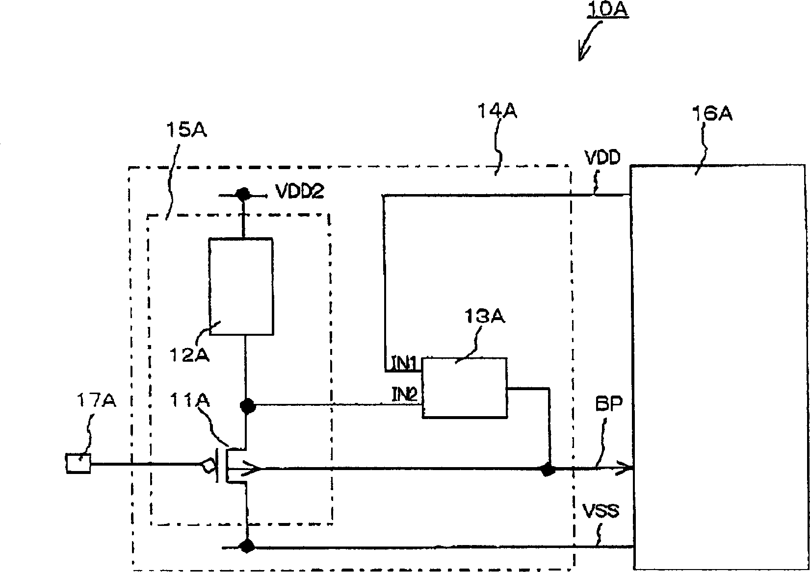
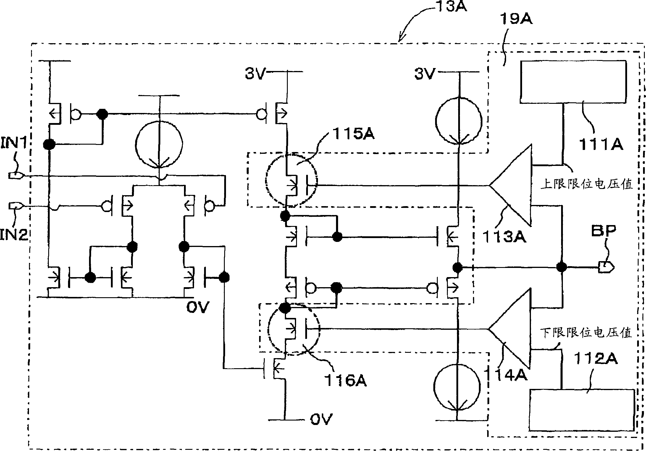
[0130] figure 1 is a circuit diagram showing a semiconductor integrated circuit device 10A related to this embodiment, as figure 1 As shown, the semiconductor integrated circuit device 10A has a monitoring device 15A, a threshold (Vth) stabilizing circuit 14A (substrate voltage adjusting device) and an integrated circuit main body 16A, wherein the monitoring device 15A is composed of a P-type MOSFET 11A and a constant current source 12A, the threshold value The (Vth) stabilizing circuit 14A (substrate voltage adjusting means) is constituted by a comparing section 13A (comparing means).
[0131] In the first embodiment, the threshold value Vth of the MOSFET is set as Vgs (gate-source voltage) when Ids=50NA×(W / L), for example, when VDD=1V. In addition, Ids is the source-drain current of the MOSFET, W is the channel width of the MOSFET, and L is the channel length of the MOSFET.
[0132] P-type MOSFET 11A is arranged on the same substrate as integrated circuit main body 16A. I...
no. 2 example
[0162] Figure 5 is a circuit diagram showing a semiconductor integrated circuit device 10B according to this embodiment. Such as Figure 5 As shown, the semiconductor integrated circuit device 10B has a monitoring device 15B, a threshold (Vth) constant circuit 14B (substrate voltage adjusting device) and an integrated circuit main body 16B, wherein the monitoring device is composed of an N-type MOSFET 11B and a constant current source 12B, and the threshold ( Vth) constant circuit 14B (substrate voltage adjusting means) is constituted by comparing section 13B (comparing means).
[0163] In the second embodiment, the threshold value Vth of the MOSFET, for example, VDD=1V, Vgs (gate-source voltage) when Ids=50NA×(W / L) is formed as Vth. In addition, Ids is the source-drain current of the MOSFET, W is the channel width of the MOSFET, and L is the channel length of the MOSFET.
[0164] N-type MOSFET 11B is arranged on the same substrate as integrated circuit body 16B. In this ...
no. 3 example
[0201] FIG. 8 is a circuit diagram showing a semiconductor integrated circuit device 20A of this embodiment.
[0202] As shown in FIG. 8, a semiconductor integrated circuit device 20A has a monitoring device 25A, a drain current (Ids) stabilizing circuit 24A (substrate voltage regulating device) and an integrated circuit main body 26A, wherein the monitoring device 25A is composed of a P-type MOSFET 21A and a constant current The source 22A is constituted, and the drain current (Ids) stabilizing circuit 24A (substrate voltage adjusting means) is constituted by a comparing part 23A (comparing means).
[0203] In the third embodiment, the saturation current of the MOSFET is taken as the source-drain current at Vgs=1V, VDD=1V, Vss=0, for example.
[0204] The drain current (Ids) constant circuit 24A is a circuit (substrate voltage regulator) for controlling the substrate voltage of the MOSFET, and stabilizes the drain current at an arbitrary gate voltage value in the saturation r...
PUM
 Abstract
Description
Claims
Application Information