Photoelectric conversion device and image pick-up system using the photoelectric conversion device

A technology for photoelectric conversion and photoelectric conversion area, which is applied in the direction of electric solid devices, parts and components of TV systems, electrical components, etc., and can solve problems such as deterioration of carrier efficiency.

Inactive Publication Date: 2004-06-16
CANON KK
View PDF1 Cites 4 Cited by
  • Summary
  • Abstract
  • Description
  • Claims
  • Application Information

AI Technical Summary

Problems solved by technology

However, here the carrier efficiency deteriorates until the desired carriers become partially extracted by the drain region

Method used


Image

  • Photoelectric conversion device and image pick-up system using the photoelectric conversion device
  • Photoelectric conversion device and image pick-up system using the photoelectric conversion device
  • Photoelectric conversion device and image pick-up system using the photoelectric conversion device

Examples


Embodiment approach 1

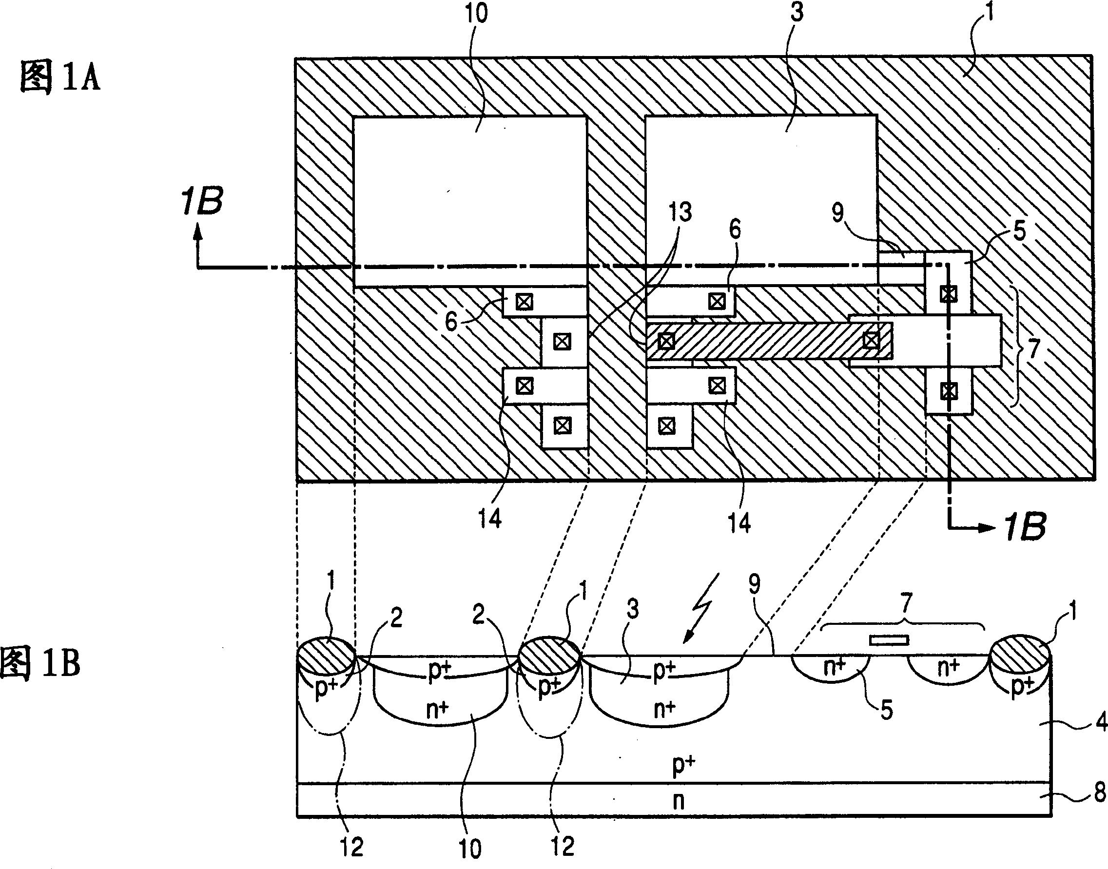
[0025] 1A is a plan view showing the configuration of a photoelectric conversion device according to a first embodiment of the present invention, and FIG. 1B is a typical cross-sectional view taken along line 1B-1B in FIG. 1A . As shown in Figures 1A and 1B, a photodiode (becoming a photoelectric conversion region) 3 is formed in the p well 4, and the charge accumulated in the photodiode 3 is due to the potential of the transfer electrode 6 becoming a high level, and the floating diffusion (floating diffusion) region 13 and the gate of the MOS transistor 7 connected to the floating diffusion region 13, and the output signal is amplified by the MOS transistor 7. Here, as shown in FIG. 1B, for the photodiode 3, the photodiode (becoming a photoelectric conversion region) 10 of an adjacent pixel is arranged via the selective oxide film 1 (surrounding the photodiodes 3 and 10). 2 is The channel blocking region (channel blocking layer) under the selective oxide film 1, 5 is the drai...

Embodiment approach 2

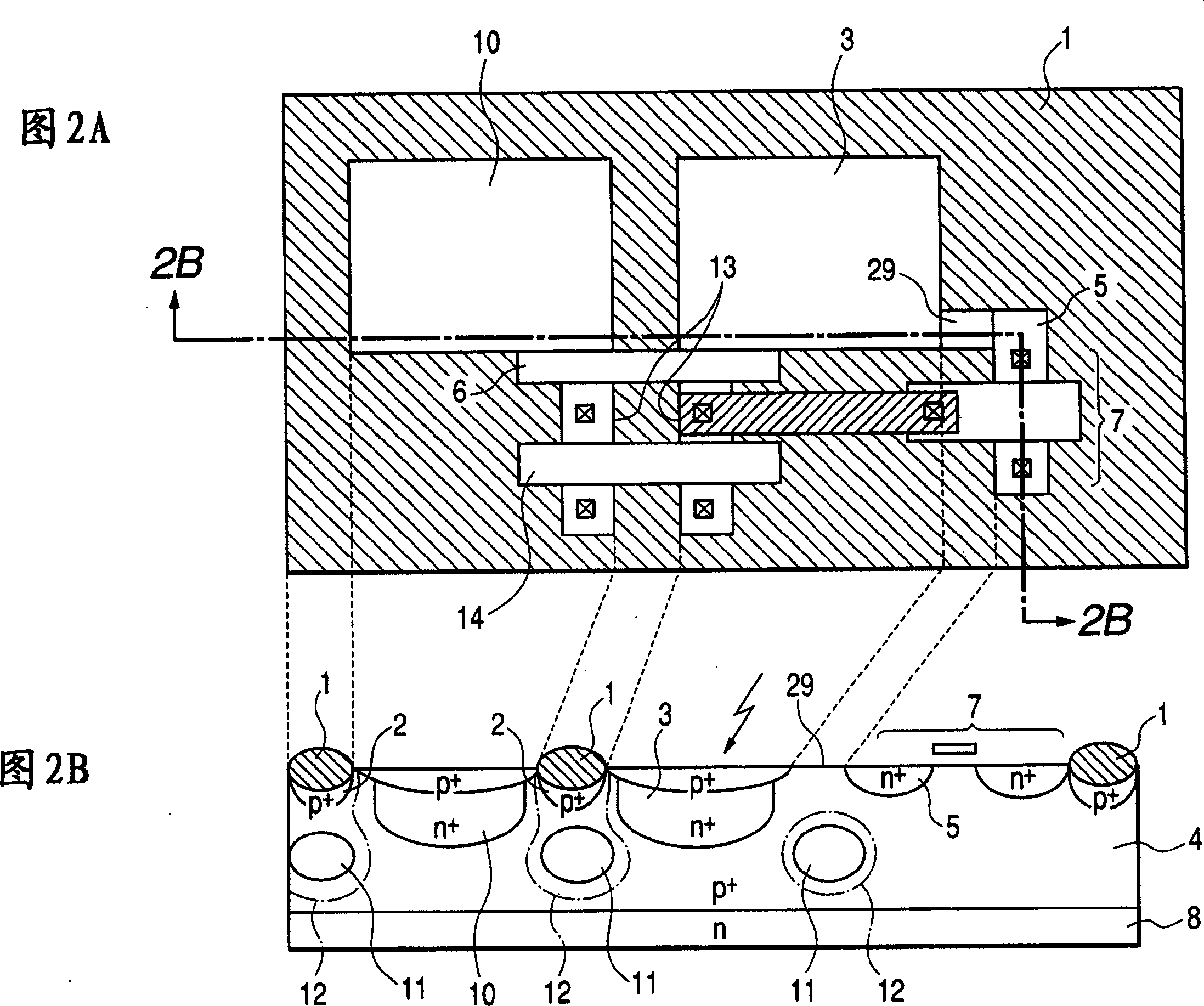
[0029] 2A is a plan view showing the configuration of a photoelectric conversion device according to a second embodiment of the present invention, and FIG. 2B is a typical cross-sectional view taken along line 2B-2B in FIG. 2A. In addition, in FIGS. 2A and 2B , the same components as those in FIGS. 1A and 1B are given the same reference numerals and their descriptions are omitted.

[0030] Compared with the first embodiment, in this embodiment, under the channel stop region 2, a p-type buried barrier layer (which will become a buried isolation region) 11 is provided to surround the photodiodes 3 and 10. . Similar to the overflow channel 9 of the first embodiment, 29 is an overflow channel as a defect region. Specifically, it is a region where the oxide film 1 and the channel stopper region 2 are not selected. In Fig. 2B, although the impurity distribution diagram is also shown, the potential distribution is a region larger than the channel stop region 2 and the barrier layer...

Embodiment approach 3

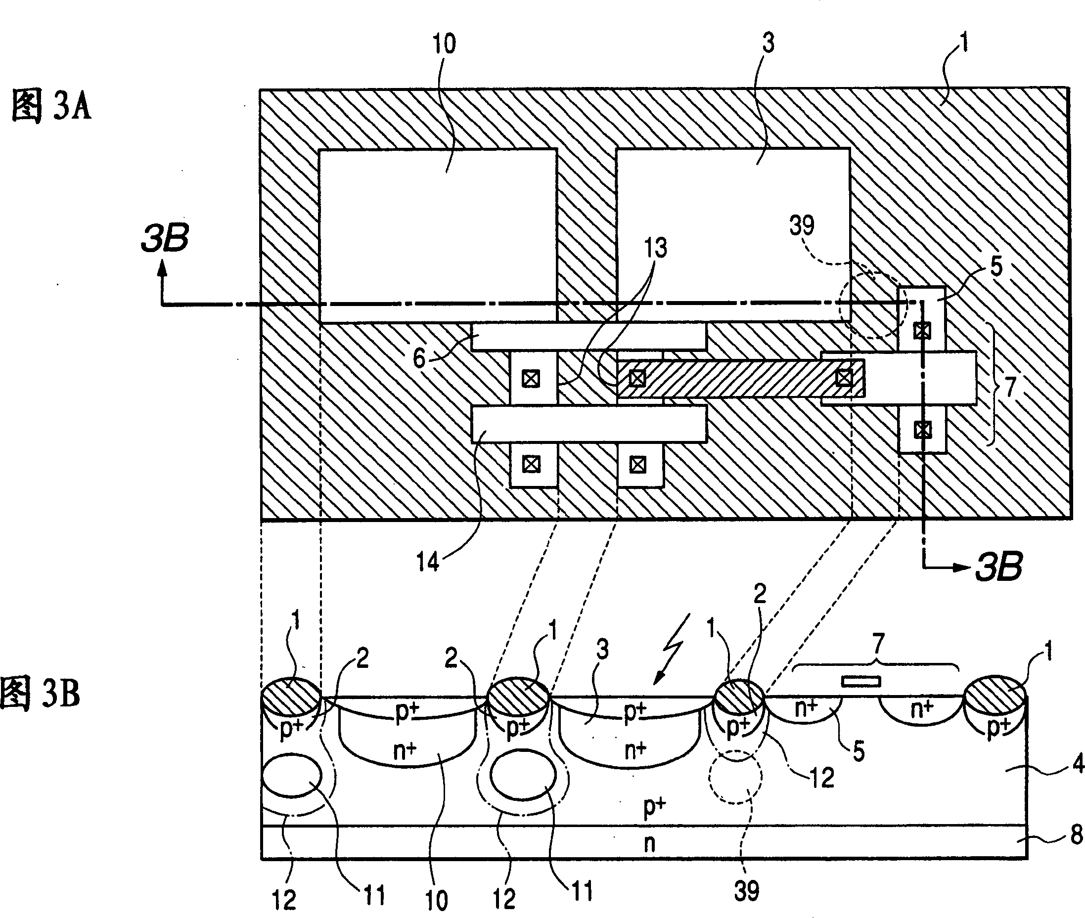
[0033] 3A is a plan view showing the configuration of a photoelectric conversion device according to a third embodiment of the present invention, and FIG. 3B is a typical cross-sectional view taken along line 3B-3B in FIG. 3A. In addition, in FIGS. 3A and 3B , the same components as those in FIGS. 2A and 2B are given the same reference numerals and their descriptions are omitted.

[0034] This embodiment is the same as Embodiment 2, the photodiodes 3 and 10 are surrounded by the buried barrier layer 11 and the surface channel stop layer 2, and only the defect region between the photodiode 3 and the drain region 5 39, no barrier layer 11 is provided.

[0035] In Fig. 3B, the distribution of the potential is a region larger than the channel blocking region 2 and the barrier layer 11, forming the respective surroundings of the channel blocking region 2 and the potential barrier layer 11, or the channel blocking region 2. A vertical wall such as the region (barrier) 12 indicated ...


PUM


Abstract

In a photoelectric conversion device with a photoelectric conversion region for accumulating electric charges that correspond to incident light and an amplifying filed effect transistor into which a signal charge from the photoelectric conversion region is inputted, the photoelectric conversion region is surrounded by a potential barrier region (a selectively oxidized film and a channel stopper), a nick region (overflow channel) is formed in a part of the potential barrier region, and a drain region of the field effect transistor that has the same conductivity type as the photoelectric conversion region is placed next to the nick region. Thus excess carriers are prevented from flowing into adjacent pixels or other floating regions.

Description

technical field [0001] The present invention relates to a photoelectric conversion device, in particular to a photoelectric conversion region which accumulates charges corresponding to incident light and a photoelectric conversion device in which signal charges from the photoelectric conversion region are input to an amplifying field effect transistor. Background technique [0002] FIG. 10A is a plan view showing the configuration of a conventional CMOS sensor, and FIG. 10B is a typical cross-sectional view taken along line 10B-10B of FIG. 10A. As shown in Figures 10A and 10B, a photodiode 1003 is formed in the p-well 1004, and the charge accumulated on the photodiode 1003 is transferred to the floating diffusion region 1011 and connected to the floating diffusion region 1011 due to the potential of the transfer electrode 1006 becoming a high level. The gate of the MOS transistor 1007 is amplified by the MOS transistor 1007 to output a signal. Here, as shown in FIG. 10B , f...

Claims


Application Information

Patent Timeline
Patent Type & Authority Applications(China)
IPC IPC(8): H01L27/146H01L27/14H01L31/00H01L31/0352H01L31/10H04N5/225H04N5/335H04N5/369H04N5/374
CPCH01L31/0352H01L27/14603H01L27/14656H01L27/1463H01L27/14609
Inventor 菊池伸
Owner CANON KK
Why Eureka
Try Eureka