Organicelectroluminescent device and its preparation method
An electroluminescent device and organic technology, applied in electroluminescent light sources, electric light sources, electrical components, etc., can solve the problems of large doping concentration error of the light-emitting layer, can no longer be adjusted, device performance is unstable, etc., and achieve good stability. The effect of sexual and luminous properties
- Summary
- Abstract
- Description
- Claims
- Application Information
AI Technical Summary
Problems solved by technology
Method used
Image
Examples
Embodiment 1
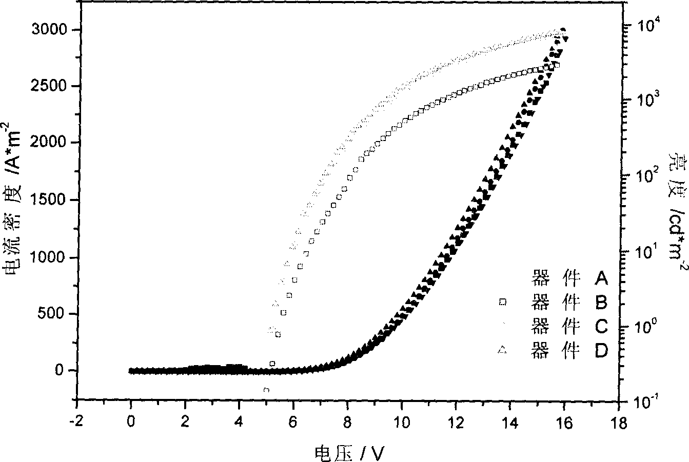
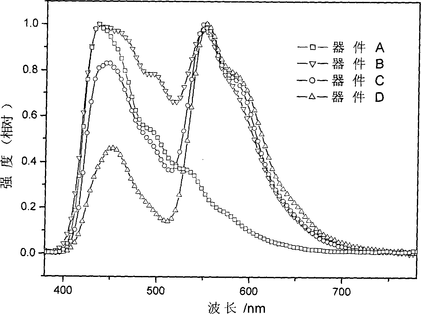
[0053] Embodiment 1: Preparation of organic electroluminescence device OLED-1 (A-D)
[0054] The glass plate coated with the ITO transparent conductive layer is ultrasonically treated in a commercial cleaning agent, rinsed in deionized water, ultrasonically degreased in acetone: ethanol mixed solvent, baked in a clean environment until the water is completely removed, and then cleaned with ultraviolet light. The light washer was irradiated for 10 minutes and the surface was bombarded with a beam of low-energy cations.
[0055] A 50 nm thick NPB hole transport layer was deposited on ITO by thermal evaporation.
[0056] Mix the solid material 99% D2NA and 1% rubrene according to the molar percentage, then melt the mixture in a container with a chemically inert environment, cool to room temperature, take out the uniform pre-doped luminescent material from the container, and put it into the evaporation source 1 , put D2NA in the evaporation source 2, control the evaporation rate ...
Embodiment 2
[0065] The glass plate coated with the ITO transparent conductive layer is ultrasonically treated in a commercial cleaning agent, rinsed in deionized water, ultrasonically degreased in acetone: ethanol mixed solvent, baked in a clean environment until the water is completely removed, and then cleaned with ultraviolet light. The light washer was irradiated for 10 minutes and the surface was bombarded with a beam of low-energy cations.
[0066] A 50 nm thick NPB hole transport layer was deposited on ITO by thermal evaporation.
[0067] Mix the solid material 99% D2NA and 1% rubrene according to the molar percentage, then melt the mixture in a container with a chemically inert environment, cool to room temperature, take out the uniform pre-doped luminescent material from the container, and put it into the evaporation source 1 , put D2NA in the evaporation source 2, control the evaporation rate of the evaporation source 1 to be 1.6% times of the evaporation rate of the evaporation...
Embodiment 3
[0072] Embodiment 3: Preparation of organic electroluminescent device OLED-2 (A-D)
[0073] The glass plate coated with the ITO transparent conductive layer is ultrasonically treated in a commercial cleaning agent, rinsed in deionized water, ultrasonically degreased in acetone: ethanol mixed solvent, baked in a clean environment until the water is completely removed, and then cleaned with ultraviolet light. The light washer was irradiated for 10 minutes and the surface was bombarded with a beam of low-energy cations.
[0074] A 50 nm thick NPB hole transport layer was deposited on ITO by thermal evaporation.
[0075] Mix the solid material 99% D2NBA and 1% rubrene according to the molar percentage, then melt the mixture in a container with a chemically inert environment, cool to room temperature, take out the uniform pre-doped luminescent material from the container, and put it into the evaporation source 1 , put D2NA in the evaporation source 2, control the evaporation rate ...
PUM
 Abstract
Description
Claims
Application Information


