
Semiconductor device

A semiconductor, high-concentration technology, applied in semiconductor devices, coupling devices, semiconductor/solid-state device manufacturing, etc., can solve problems such as deterioration of high-frequency characteristics, achieve electrostatic energy attenuation, prevent electrostatic damage, and protect FETs

Inactive Publication Date: 2004-08-11
SANYO ELECTRIC CO LTD
View PDF0 Cites 7 Cited by
  • Summary
  • Abstract
  • Description
  • Claims
  • Application Information

AI Technical Summary

Problems solved by technology

However, in microwave devices, this method cannot be used because the connection of the protection diode increases the parasitic capacitance and deteriorates the high-frequency characteristics.

Method used


Image

  • Semiconductor device
  • Semiconductor device
  • Semiconductor device

Examples


Embodiment Construction

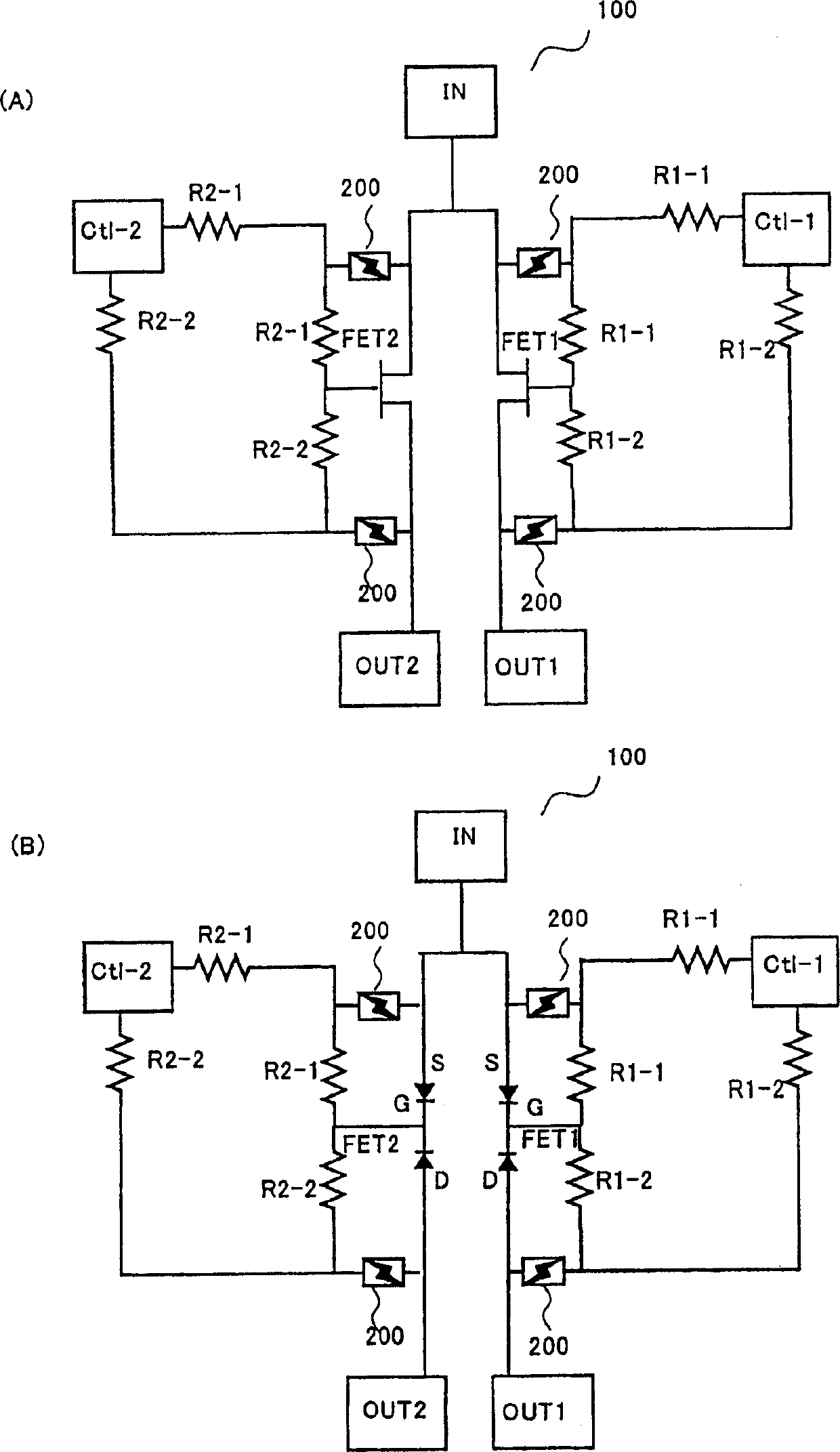
[0084] An embodiment of the present invention will be described in detail using FIGS. 1 to 22 .

[0085] FIG. 1 is a circuit diagram showing a compound semiconductor switching circuit device 100 of a device to be protected. The source electrodes (or drain electrodes) of the first FET1 and the second FET2 are connected to the common input terminal IN, and the gates of the FET1 and FET2 are respectively connected to the first and second control terminals Ctl-1 and Ctl- through resistors R1 and R2. 2. In this way, the drain electrodes (or source electrodes) of FET1 and FET2 are connected to the first and second output terminals OUT1 and OUT2. The control signals applied to the first and second control terminals Ctl-1 and Ctl-2 are complementary signals, and the FET on the side to which the H level signal is applied is turned on, so that the signal applied to the common input terminal IN is transmitted to either output terminal. input signal.

[0086]The DC potential of the resi...


PUM


Abstract

To solve the problem wherein a method cannot be used because the increase of a parasitic capacitance, due to the connection of a protection diode, causes deterioration in the high-frequency characteristics in a microwave device, even though a method for connecting an electrostatic breakdown protective diode, in parallel with the both ends of a p-n junction and a Schottky junction which exist within a device and is apt to be broken electrostatically, can be considered in order to generally protect the device against static electricity. Two pathways, from a gate electrode pad to a gate electrode on an operating region, are provided in parallel, and one path passes through, in the vicinity of a source electrode pad and the other passes through in the vicinity of a drain electrode pad. Protective elements, arranged respectively adjacently, are connected between the gate electrode and the source electrode, or the gate electrode and the drain electrode. Consequently, electrostatic breakdown voltage of a FET can be improved from about 100V to 700V.

Description

technical field [0001] The present invention relates to a semiconductor device, and more particularly to a semiconductor device in which the electrostatic breakdown voltage is greatly improved. Background technique [0002] The microwave equipment market for general consumer use, which started with the appearance of satellite broadcasting receivers, has expanded rapidly due to the worldwide spread of mobile phones. Now, the market for wireless broadband applications has really begun. In these markets, gallium-arsenic (GaAs) devices suitable for microwave use are mainly used, and conventional Si devices are refined and three-dimensionally structured to achieve low parasitic capacitance and low parasitic resistance Si microwave devices. [0003] Fig. 23 is a circuit diagram showing a compound semiconductor switching circuit device. The source electrodes (or drain electrodes) of the first FET1 and the second FET2 are connected to the common input terminal IN, and the gate elec...

Claims


Application Information

Patent Timeline
Patent Type & Authority Applications(China)
IPC IPC(8): H01L27/04H01L21/338H01L21/822H01L23/48H01L23/52H01L23/60H01L23/62H01L27/02H01L29/812H03K17/00H03K17/08
CPCH01L27/0288H01L24/05H01L2924/12032H01L29/812H01L2924/13055H01L2924/12036H01L2924/13063H01L2924/13091H01L2924/00H04B1/40H04M1/6066H01R31/06
Inventor 浅野哲郎榊原干人平井利和
Owner SANYO ELECTRIC CO LTD
Learn More