Two-bit ROM unit of nitride and its manufacture and read method
A technology of read-only storage and manufacturing method, which is applied in the field of two-bit nitride read-only memory cells, and can solve problems such as the increase of the critical voltage of the memory cell and the inability to open the channel 26
- Summary
- Abstract
- Description
- Claims
- Application Information
AI Technical Summary
Problems solved by technology
Method used
Image

Examples
Embodiment Construction
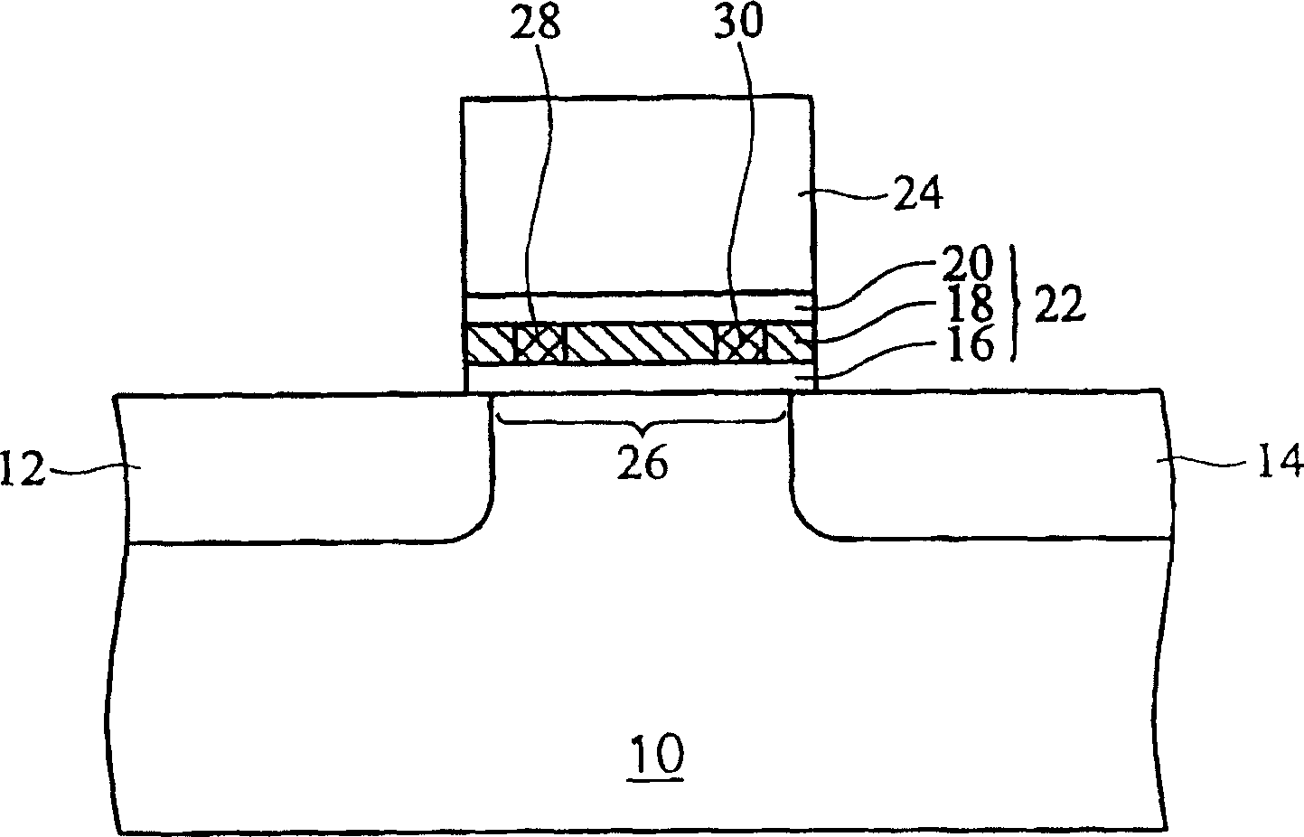
[0035] Manufacturing method and structure of a two-bit nitride read-only memory cell with a parasitic amplifier:
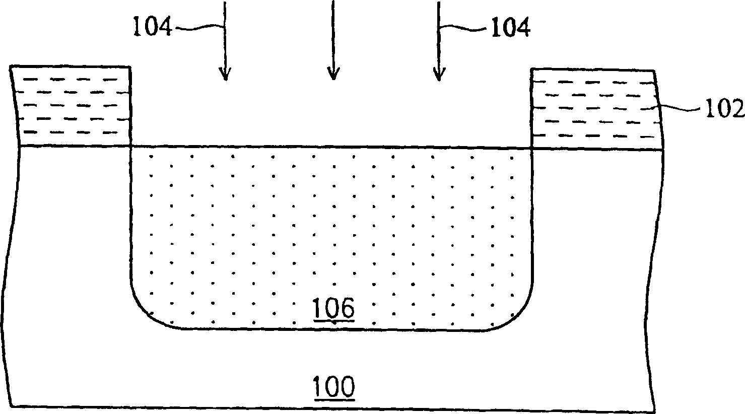
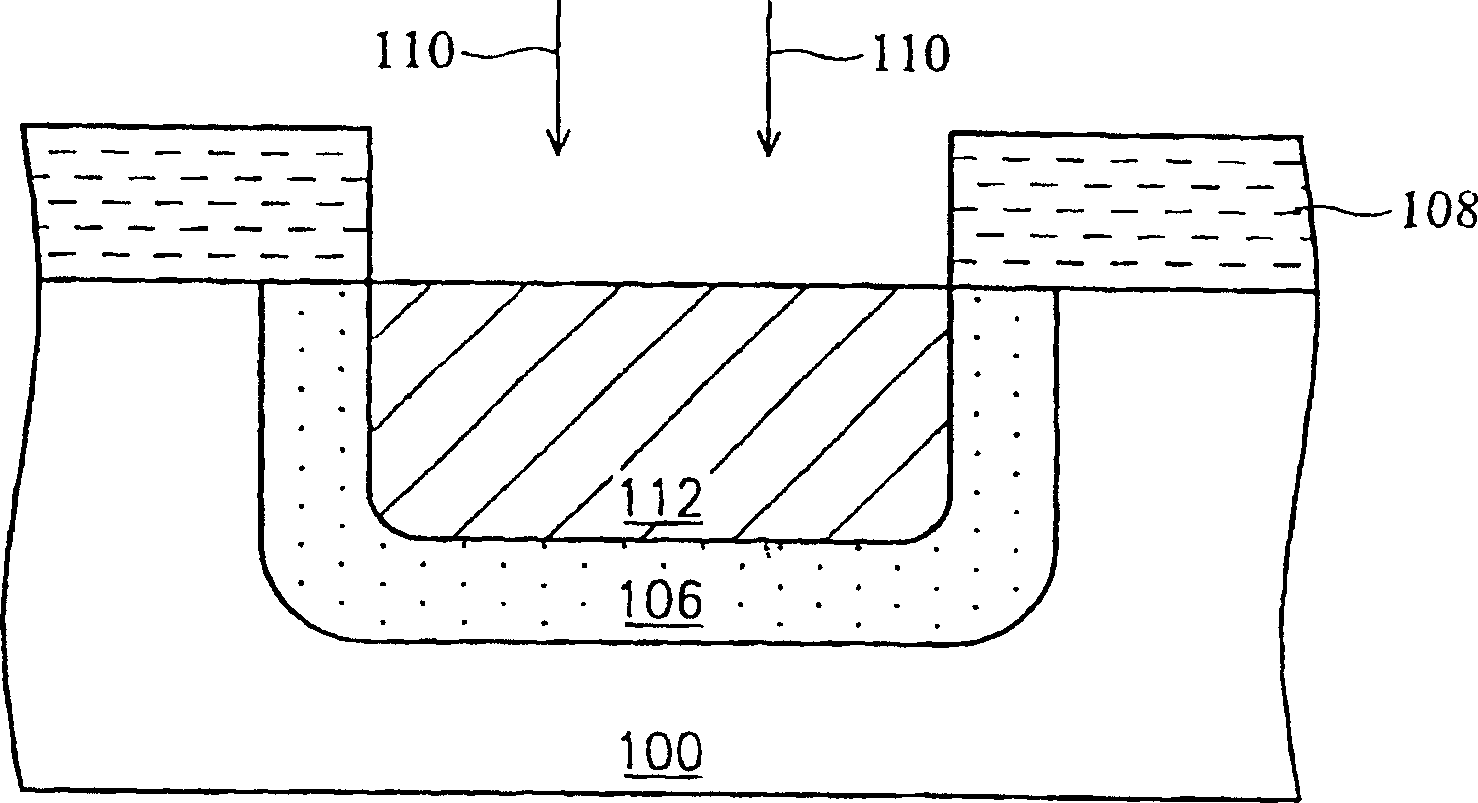
[0036] The manufacturing method of the two-bit nitride read-only memory cell with parasitic amplifier of the present invention will cooperate with Figure 2 to Figure 7 Make a detailed description as follows. At figure 2 In this method, firstly, a semiconductor substrate is provided, for example, a silicon substrate 100 made of p-type silicon material here. Next, a masking layer 102 is formed on the surface of the silicon substrate 100 to define the memory cell area, and its material is, for example, photoresist (PR). Then perform an ion implantation process 104 and use the above-mentioned shielding layer 102 as an ion implant mask (implant mask), implant n-type ions such as phosphorus (P) with an energy between 300-2000KeV to form an ion in the silicon substrate 100. The first well region 106, the first well region 106 is an n-type well region doped with n-ty...
PUM
 Abstract
Description
Claims
Application Information
 - R&D Engineer
- R&D Manager
- IP Professional
- Industry Leading Data Capabilities
- Powerful AI technology
- Patent DNA Extraction
Browse by: Latest US Patents, China's latest patents, Technical Efficacy Thesaurus, Application Domain, Technology Topic.
© 2024 PatSnap. All rights reserved.Legal|Privacy policy|Modern Slavery Act Transparency Statement|Sitemap