Base board for optical mask, optical mask blank and optical mask

A photomask and substrate technology, which is applied in the field of large photomask substrates, can solve the problems of increased substrate weight, inability to handle photomasks safely, and easy slipping of side parts

Active Publication Date: 2004-09-29
HOYA CORP
View PDF1 Cites 9 Cited by
  • Summary
  • Abstract
  • Description
  • Claims
  • Application Information

AI Technical Summary

Problems solved by technology

However, during the manufacture and use of photomasks, people usually carry the side of the substrate by hand, but due to the increasing size, the weight of the substrate is also increasing (about 1Kg to 15Kg). , need to be very careful when handling by hand
In such a case, if the side surface is a mirror surface, the side surface will be very slippery, which increases the risk of the mask slipping when being transported by hand, and thus there is a serious problem that the photomask cannot be handled safely.

Method used


Image

  • Base board for optical mask, optical mask blank and optical mask
  • Base board for optical mask, optical mask blank and optical mask
  • Base board for optical mask, optical mask blank and optical mask

Examples


Embodiment approach 1

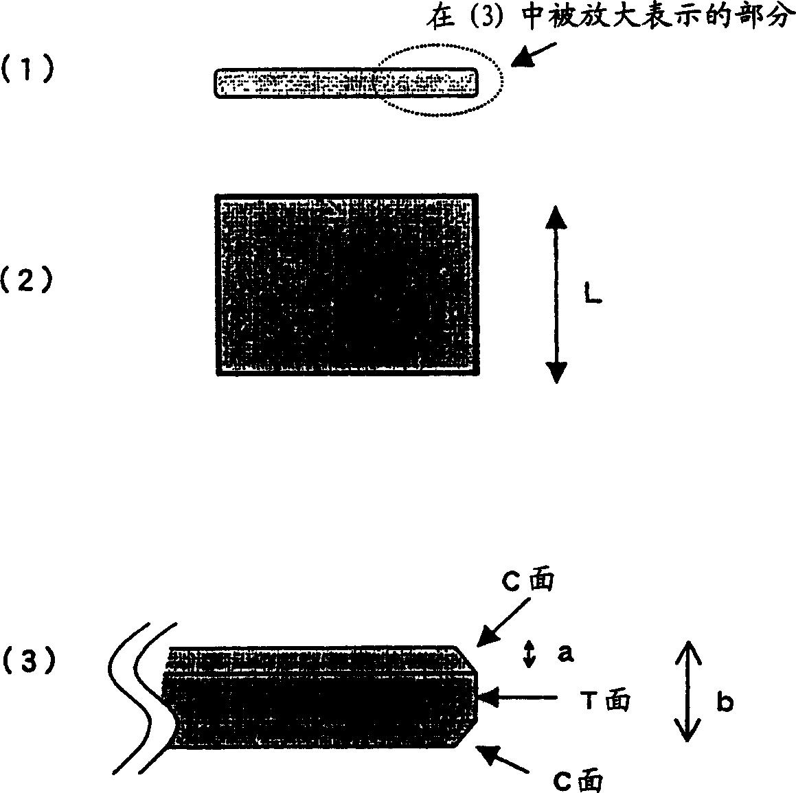
[0036] In the substrate for a large photomask described in Embodiment 1, the chamfered surface (C surface) and the end surface (T surface) constituting the side portion of the substrate for a large photomask are formed with a surface roughness on the entire circumference of the substrate. (Ra) is a rough surface of 0.03 to 0.3 μm.

[0037] Here, if the surface roughness (Ra) of the C surface and the T surface is less than 0.03 μm, it is easy to slip, and there is a danger of slipping at any time when picked up by hand. In addition, when the surface roughness (Ra) of the C surface and the T surface exceeds 0.3 μm, particles generated from the side surfaces are conspicuous.

[0038] The lower limit of the surface roughness (Ra) of the C surface and the T surface is preferably equal to or greater than 0.05 μm, more preferably equal to or greater than 0.1 μm, and most preferably equal to or greater than 0.15 μm. The upper limit of the surface roughness (Ra) of the C surface and t...

Embodiment 1

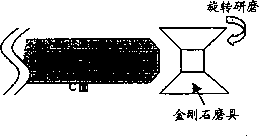
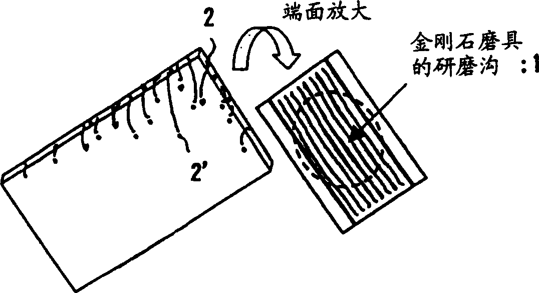
[0047] The side surfaces (C surface and T surface) of the substrate for a photomask were ground along the entire circumference of the substrate using a diamond grinder with a grain size of #800. The side surfaces (C surface and T surface) were polished to a rough surface with Ra of 0.2 μm. This surface is an opaque translucent surface when viewed visually. Here, the surface roughness Ra is measured on a line of about 10 mm at an arbitrary location of the side surface.

[0048] The photomask blank on which the light-shielding film was formed on the substrate was soaked and cleaned. Then, the surface of the cleaned photomask blank was inspected for foreign matter, and it was found that almost no particles that may be generated from the side surface of the substrate were detected.

[0049] Moreover, this board does not cause a problem particularly when it is picked up by hand.

Embodiment approach 2

[0051] In the substrate for a large photomask described in Embodiment 2, the chamfered surface (C surface) and the end surface (T surface) constituting the side portion of the substrate for a large photomask are formed on the entire circumference of the substrate, and the above-described The end surface T is formed as a rough surface, and the chamfered surface C is formed as a rough surface with a surface roughness smaller than that of the end surface.

[0052] Here, by making the chamfered surface C a rough surface smaller than the surface roughness of the end surface, there are the following advantages.

[0053] First, in the process of cleaning the substrate, photomask blank, and photomask, in addition to (1) so-called immersion cleaning in which the substrate is immersed in a cleaning solution, and (2) so-called spin cleaning in which the substrate is rotated while supplying the cleaning solution, There is also (3) so-called scrub cleaning in which the surface of the subst...


PUM

PropertyMeasurementUnit
thicknessaaaaaaaaaa
thicknessaaaaaaaaaa
thicknessaaaaaaaaaa

Abstract

A substrate for photomask has a top surface and a back surface, the substrate being square in shape, an end surface formed along the thickness thereof and a chamfered surface formed on a perimeter edge region where the end surface and the top surface meet and another region where the end surface and the back surface meet, a size of the perimeter edge of the substrate is 300 mm or more on a side and the end surface and the chamfered surface each has a roughened surface having a surface roughness (Ra) ranging from 0.03 mum to 0.3 mum.

Description

technical field [0001] The present invention relates to a substrate for a large photomask used for pattern replication in photolithography when manufacturing a display device. Background technique [0002] A photomask for forming a light-shielding film pattern on a light-transmitting substrate is known. The substrate used for this photomask is a substrate made of synthetic quartz glass or the like and has a rectangular surface shape. However, the surface is generally mirror-polished in consideration of light scattering when the photomask is used. In addition, Patent Document 1 discloses a method to prevent debris remaining in the grinding groove on the side surface from adhering to the surface during the production of the photomask to form impurity defects, etc., which will adversely affect the quality. , The technique of mirror-polishing the side surface (end surface and chamfer surface) of the substrate. [0003] (Patent Document 1: JP-A-56-46227) [0004] In addition, ...

Claims


Application Information

Patent Timeline
Patent Type & Authority Applications(China)
IPC IPC(8): H01L21/027C03C19/00C03C23/00G03F1/00G03F1/60G03F7/20G03F9/00H01L21/00
CPCC03C2204/08C03C19/00C03C23/0075G03F1/14G03F1/60G03F1/50G03F1/62
Inventor 大田黑竜桥口浩一
Owner HOYA CORP
Why Eureka
Try Eureka