Method for manufacturing low-temperature polysilicon thin-film transistor

A low-temperature polysilicon and thin-film transistor technology, which is applied in semiconductor/solid-state device manufacturing, electrical components, circuits, etc., to achieve good moisture resistance, improve electrical characteristics, and high insulation strength

Inactive Publication Date: 2005-01-19
TPO DISPLAY
View PDF0 Cites 12 Cited by
  • Summary
  • Abstract
  • Description
  • Claims
  • Application Information

AI Technical Summary

Problems solved by technology

[0014] However, in the above-mentioned various existing technologies, none of the technical solutions can produce a composite material with good interface properties and high threshold voltage stability, and has better barrier and anti-blocking capabilities for water vapor and metal ions. , and low temperature polysilicon thin film transistors with high breakdown voltage

Method used


Image

  • Method for manufacturing low-temperature polysilicon thin-film transistor
  • Method for manufacturing low-temperature polysilicon thin-film transistor
  • Method for manufacturing low-temperature polysilicon thin-film transistor

Examples


Embodiment Construction

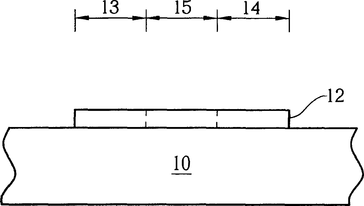
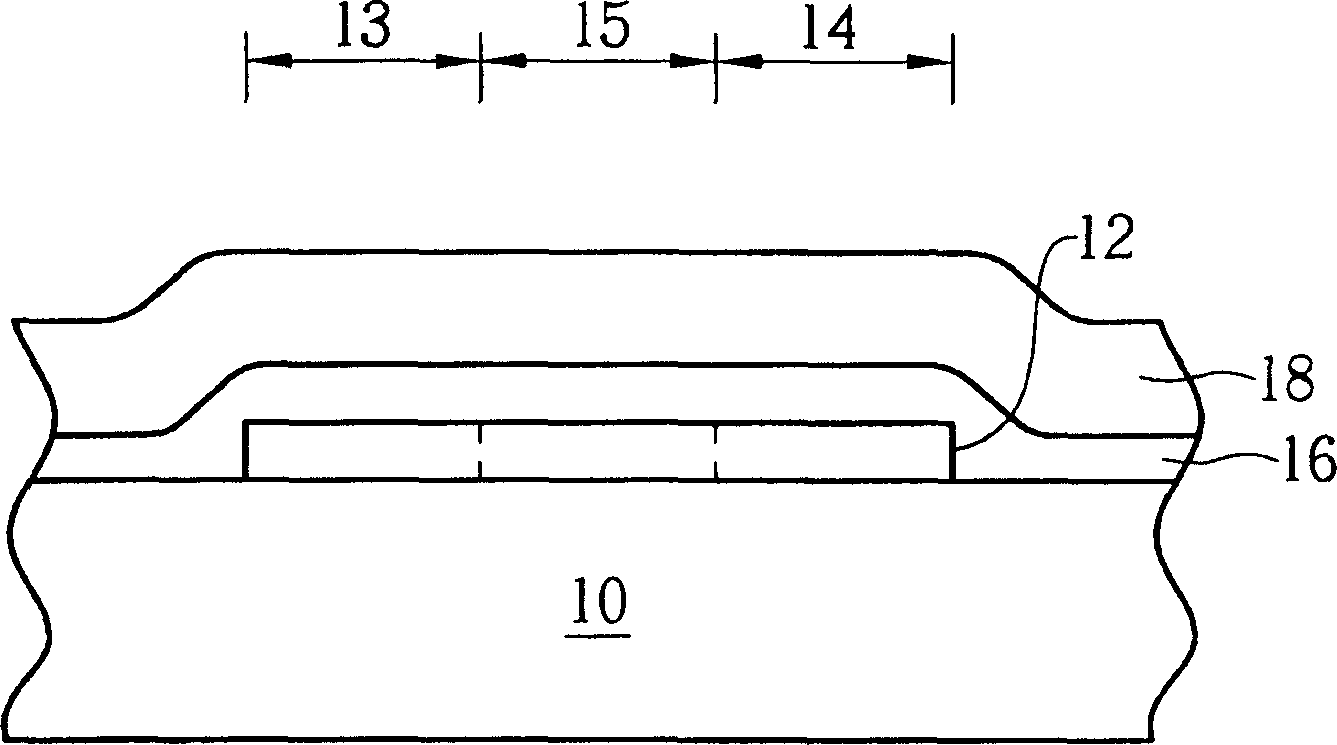
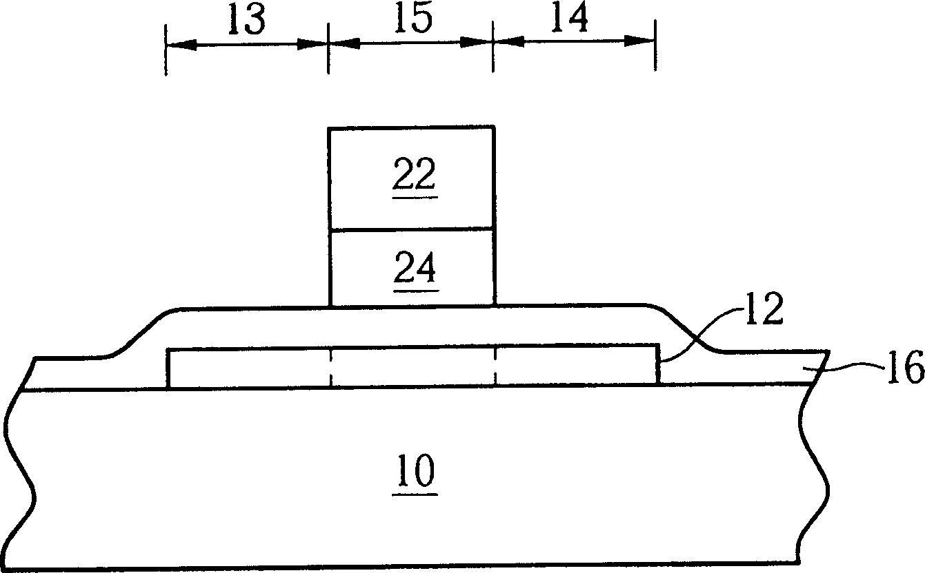
[0051] Please refer to Figure 7 to Figure 10 , Figure 7 to Figure 10 It is a schematic diagram of a method for manufacturing a low temperature polysilicon thin film transistor (LTPSTFT) 122 according to the first embodiment of the present invention. like Figure 7 As shown, the low temperature polysilicon thin film transistor of the present invention is fabricated on an insulating substrate 100. The insulating substrate 100 must be made of a transparent material, usually a glass substrate or a quartz substrate. First, an amorphous silicon thin film (amorphous silicon thin film, α-Si thin film, not shown) is formed on the surface of the insulating substrate 100, and then an excimer laser annealing (excimer laser annealing, ELA) process is performed to make the amorphous silicon thin film The silicon film (not shown) is recrystallized (recrystallize) to become a polysilicon layer 102, and the surface of the polysilicon layer 102 includes a source region (source region) 103, ...


PUM

PropertyMeasurementUnit
thicknessaaaaaaaaaa
thicknessaaaaaaaaaa

Abstract

The invention relates to a method of making low temperature polycrystalline silicon thin film transistor (LTPS TFT), firstly forming a polycrystalline silicon layer containing a channel region, successively making first and second plasma enhancement chemical gas phase deposition procedures so as to in sequence form a silicon oxide layer with tetraethyl silicon hydroxide as the principal and a compound grid insulating layer composed of a silicon nitride layer, and finally forming a grid electrode and source/drain of the LTPS TFT.

Description

technical field [0001] The present invention relates to a method for manufacturing a low temperature polysilicon thin film transistor (LTPS TFT), in particular to a method for manufacturing a low temperature polysilicon thin film transistor with excellent electrical characteristics and reliability. Background technique [0002] Among today's flat panel display technologies, liquid crystal display (LCD) can be said to be the most mature technology. For example, mobile phones, digital cameras, video cameras, notebook computers and even monitors that are common in daily life are Products manufactured using this technology. However, with the improvement of people's requirements for display visual experience and the continuous expansion of new technology application fields, flat-panel displays with higher image quality, high definition, high brightness and low price have become the trend of future display technology development. The driving force behind the development of new di...

Claims


Application Information

Patent Timeline
Patent Type & Authority Applications(China)
IPC IPC(8): H01L21/336H01L21/84
Inventor 林辉巨
Owner TPO DISPLAY
Why Eureka
Try Eureka