Semiconductor device and display device
A technology for semiconductors and power lines, applied in the fields of semiconductor devices and display devices, can solve problems such as increased current consumption, and achieve the effects of reducing costs, reducing actual installation steps and actual installation areas, and reducing manufacturing costs.
- Summary
- Abstract
- Description
- Claims
- Application Information
AI Technical Summary
Problems solved by technology
Method used
Image
Examples
no. 1 approach
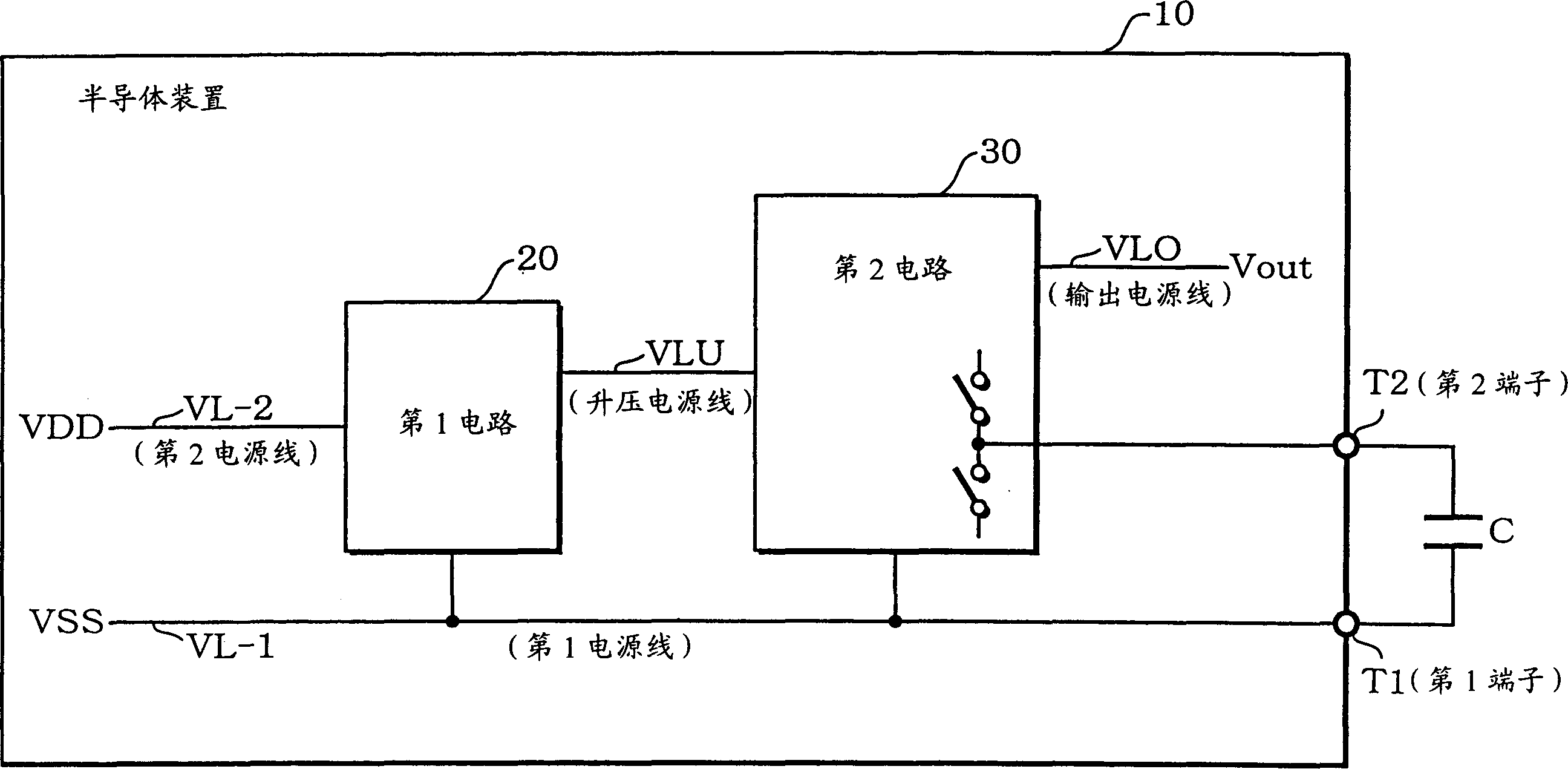
[0081] figure 1 is a schematic configuration diagram of the semiconductor device in the first embodiment. The semiconductor device (integrated circuit device (IC), chip) 10 is used to boost the voltage between the first and second power supply lines VL-1 and VL-2 to M×N (M>N, M, N is positive Integer) times to generate the output voltage Vout. The output voltage Vout is output between the first power supply line VL-1 and the output power supply line VLO.
[0082] The semiconductor device 10 includes first and second circuits 20, 30 and first and second terminals T1, T2.
[0083] The first circuit 20 is connected to the first and second power supply lines VL-1, VL-2 and the boosted power supply line VLU. Moreover, the first circuit 20 operates according to the charge pump (Charge Pump), and outputs the voltage M·V obtained by multiplying the voltage VM between the first and second power supply lines VL-1 and VL-2 to the first power supply line. Between VL-1 and the boost po...
PUM
 Abstract
Description
Claims
Application Information


