Plasma production of polycrystalline silicon

a technology of polycrystalline silicon and polycrystalline silicon, which is applied in the direction of silicon compounds, chemical/physical/physical-chemical processes, energy-based chemical/physical/physical-chemical processes, etc., to achieve the effects of lowering the cost of producing semiconductor grade silicon, reducing containment costs, and high condensation temperatures

Inactive Publication Date: 2005-08-09
TENOROC
View PDF6 Cites 23 Cited by
  • Summary
  • Abstract
  • Description
  • Claims
  • Application Information

AI Technical Summary

Benefits of technology

[0009]In another embodiment of the invention, a chlorine based system is used to produce polysilicon from SiCl4. This system functions in the same way as the fluorine based system while allowing higher condensation temperatures and lower containment costs.
[0010]These embodiments represent a transfer of silicon from SiO2 to polysilicon without the production of metallurgical grade silicon. These embodiments have the advantage of eliminating the need of producing MGS as a precursor in the production of polysilicon, significantly lowering the cost of producing semiconductor grade silicon. The cost is further lowered over the prior art procedures as the entire operation can be contained in one facility which will lower the costs of operating multiple facilities. Additionally, these processes consume by products in a continuous manner, and are therefore environmentally friendly.

Problems solved by technology

This is expensive and often requires the separation of the different processing steps into different facilities or locations.

Method used


Image

  • Plasma production of polycrystalline silicon
  • Plasma production of polycrystalline silicon
  • Plasma production of polycrystalline silicon

Examples


Embodiment Construction

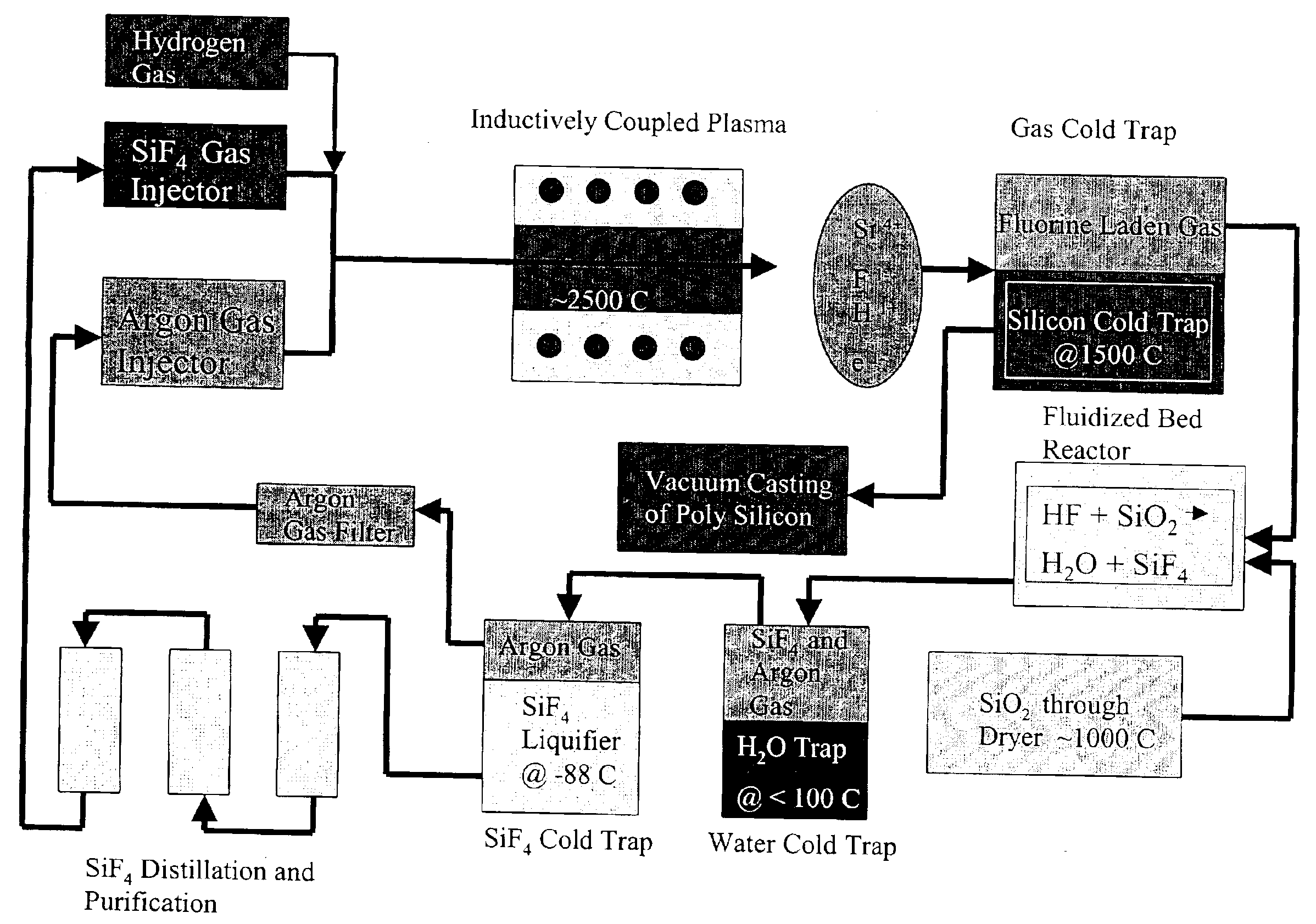
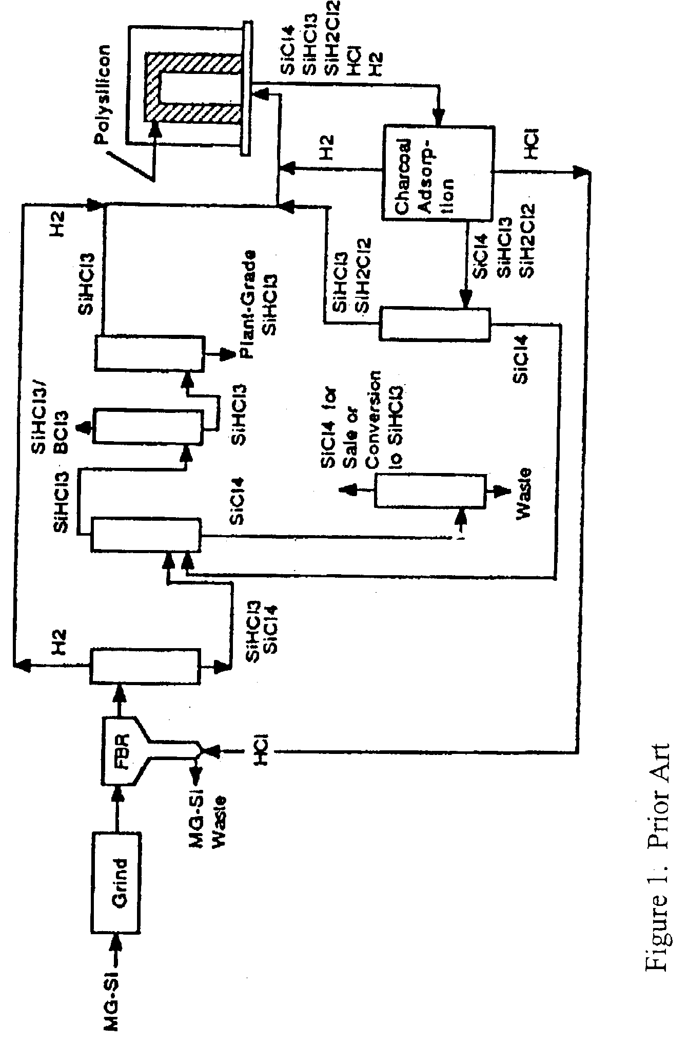
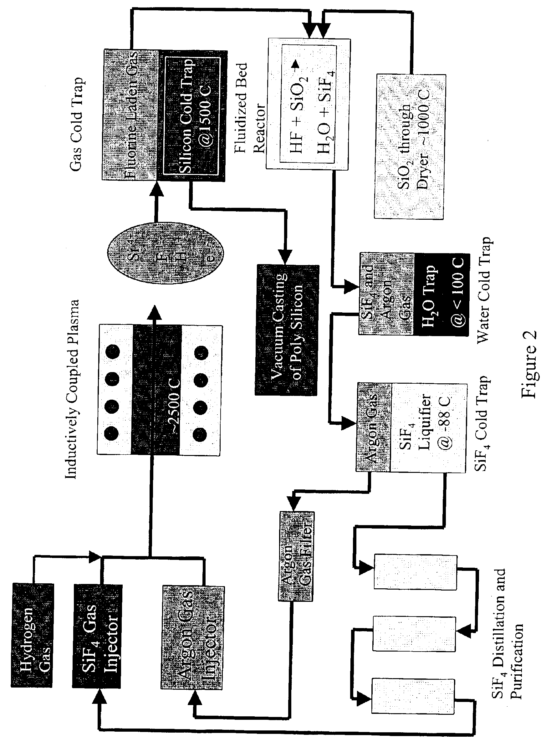
[0017]The present invention encompasses a method of transferring silicon from SiO2 to polysilicon without the production of metallurgical grade silicon or the use of a metallurgical grade silicon intermediate. The invention is embodied in a process utilizing an inductively coupled plasma in the presence of hydrogen to break down a silicon halide and the subsequent reformation of the silicon halide via the reaction between the halide gas and silica feedstock in a fluidized bed reactor.

[0018]In one embodiment of the invention, the process features a fluorine based system. Referring to FIG. 2, SiF4, hydrogen and argon are injected into an inductively coupled plasma operating at a temperature of approximately 2500° C. A plasma is defined as a luminous gas containing a significant fraction of ionized atoms or molecules. Plasmas, therefore, are considered to be gaseous conductors. As such, plasmas readily interact with magnetic fields, making it possible to couple a plasma to a high frequ...


PUM

PropertyMeasurementUnit
temperatureaaaaaaaaaa

Abstract

The invention is directed to a method of producing polycrystaline silicon metal from a silicon halide plasma source. The silicon halide is split into silicon and halide ions in an inductively coupled plasma and silicon ions are then condensed to form molten silicon metal that can be vacuum cast into polysilicon ingots. The halide ions are separated and recycled into silicon halide gas over a silicon dioxide bed. In this way, high grade polysilicon is produced without a metallurgical grade silicon precursor and the process these processes consumes the byproducts in a continuous manner madding it less expensive than traditional methods of producing polysilicon and more environmentally friendly.

Description

CROSS REFERENCE TO RELATED APPLICATIONS[0001]This application claims benefit under 35 USC § 119(e) of U.S. Provisional Application No. 60 / 348,939, filed Jan. 17, 2002, which is incorporated herein in its entirety by this reference.TECHNICAL FIELD OF THE INVENTION[0002]The invention is directed to a method of producing semiconductor grade silicon from a silicon halide plasma source followed by condensation of silicon ions to form molten silicon metal.BACKGROUND OF THE INVENTION[0003]Crystal growth is a very orderly and regulated process. Often many small crystals begin forming in solution and grow until their edges meet at varying angles. They do not join to form a single large crystal but rather remain a mass of small individual crystals forming a polycrystalline mass. Polycrystalline silicon metal (polysilicon) is a precursor to the manufacture of silicon single crystals used extensively in the microelectronics industry. Most of the current manufacturing schemes for the production ...

Claims


Application Information

Patent Timeline
Patent Type & Authority Patents(United States)
IPC IPC(8): B01J19/08C01B33/027C01B33/00H01L21/205H01L21/02
CPCB01J19/088C01B33/027H01L21/02532H01L21/0262H01L21/02661B01J2219/00006B01J2219/0883B01J2219/0894
Inventor KELSEY, PAUL V.
Owner TENOROC
Why Eureka
Try Eureka