Methods of manufacturing wiring pattern, methods of manufacturing organic electro luminescent element

A manufacturing method and thin-film pattern technology, which is applied in the manufacture of electroluminescent light sources, discharge tubes/lamps, ships or lead-in wires, etc., can solve the problem of uneven film thickness, time-consuming, and uneven light emission of thin-film patterns, etc. problem, achieve the effect of reducing uneven lighting

Active Publication Date: 2005-02-02
KATEEVA DISPLAY TECH (SHAOXING) LTD
View PDF1 Cites 5 Cited by
  • Summary
  • Abstract
  • Description
  • Claims
  • Application Information

AI Technical Summary

Problems solved by technology

[0013] When such streaky unevenness occurs, the film thickness of the thin film pattern becomes uneven, so when the thin film pattern is used as, for example, a hole injection layer of a pixel, a light emitting layer, or a color filter, streaks are generated uneven light emission
[0014] In addition, in the formation of thin film patterns constituting pixels using the conventional droplet discharge method, since one ink nozzle is used to discharge liquid droplets in one scan of one pixel area, there is a need for The problem that it takes a lot of time to form the thin film pattern

Method used


Image

  • Methods of manufacturing wiring pattern, methods of manufacturing organic electro luminescent element
  • Methods of manufacturing wiring pattern, methods of manufacturing organic electro luminescent element
  • Methods of manufacturing wiring pattern, methods of manufacturing organic electro luminescent element

Examples


Embodiment approach 1

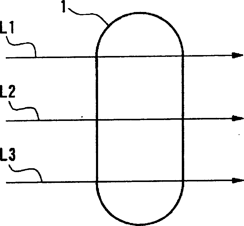
[0073] figure 1 It is an explanatory drawing showing the manufacturing method of the thin film pattern in Embodiment 1 of this invention. A pixel region 1 is formed on a substrate. It is preferable to provide rib-shaped partition walls (banks) on the outer periphery of the pixel area 1 . The pixel area 1 takes a longitudinal shape, with a long axis passing through the center of the pixel area 1 and running vertically through the pixel area 1 , and a short axis passing through the center of the pixel area 1 and running across the pixel area 1 . Furthermore, the shape of the pixel area 1 may be rectangular, elliptical, or the like.

[0074] In the pixel area 1, a liquid material is applied by ejecting droplets. For example, when the pixel formed in the pixel region 1 is an organic EL element, the liquid material is a material composed of a material for forming a hole injection layer or a light emitting layer and a solvent. figure 1The illustrated scanning lines L1 , L2 , a...

Embodiment approach 2

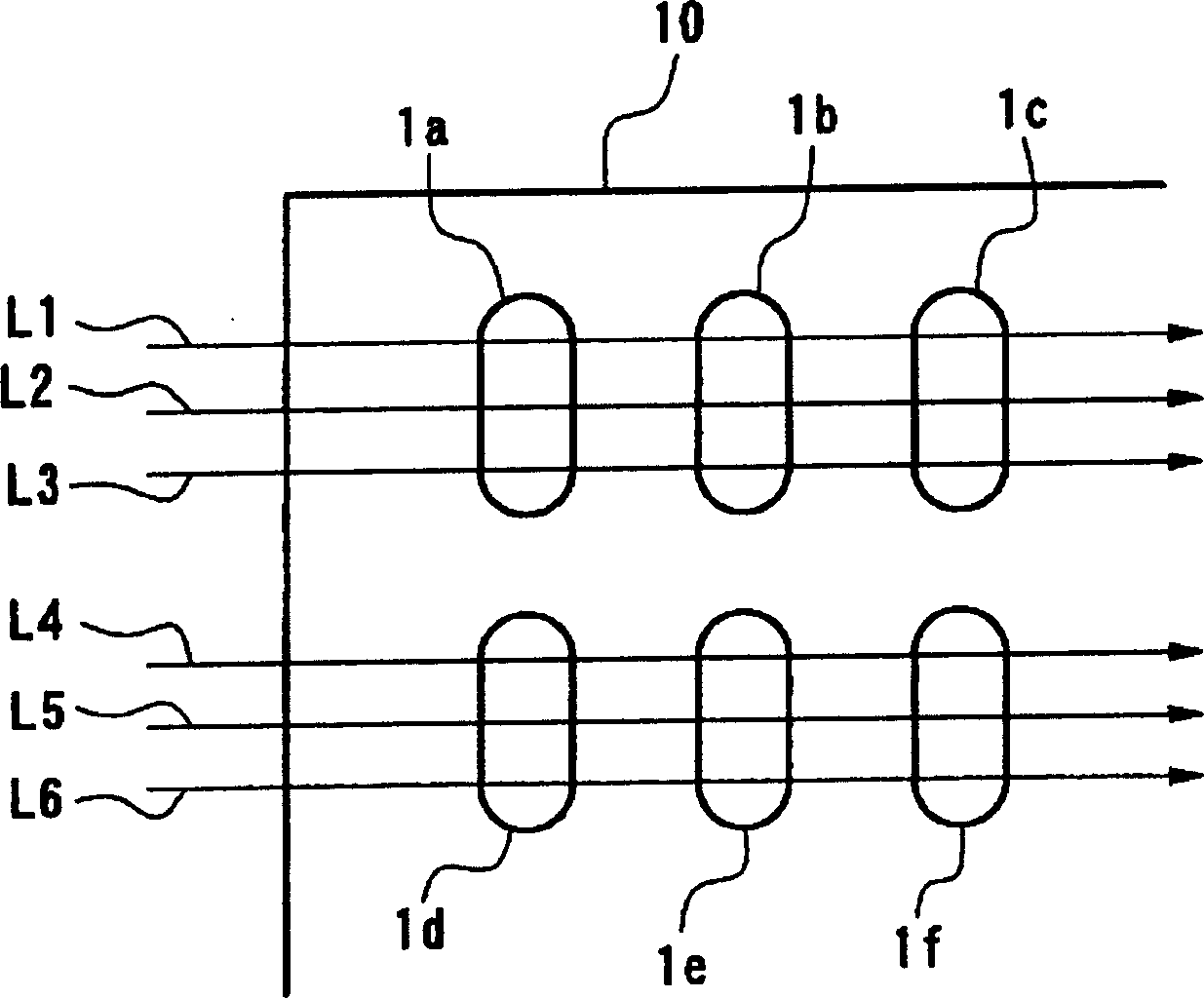
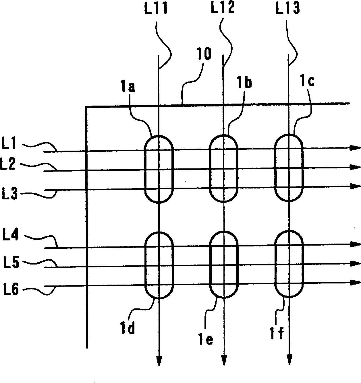
[0094] Refer below image 3 Embodiment 2 of the present invention will be described. image 3 It is an explanatory drawing showing the manufacturing method of the thin film pattern in Embodiment 2 of this invention. The difference between this embodiment and the above-mentioned Embodiment 1 is that in this embodiment, not only the scanning lines L1, L2, L3, L4, L5, L6, and scanning lines L11, L12, L13 are set along the long-axis directions of the pixel regions 1a, 1b, 1c, 1d, 1e, and 1f.

[0095] Specifically, first, a plurality of pixel regions 1 a , 1 b , 1 c , 1 d , 1 e , and 1 f are formed on the upper surface of the substrate 10 . It is preferable to provide rib-shaped partitions (dams) on the outer peripheries of the respective pixel regions 1a, 1b, 1c, 1d, 1e, and 1f.

[0096] Thereafter, for the pixel regions 1a, 1b, 1c formed as pixels of the first row, and figure 2 The method shown is the same, the scanning lines L1, L2, L3 are set, and the ink nozzles are scann...

Embodiment approach 3

[0101] Refer below Figure 4 and Figure 5 Embodiment 3 of the present invention will be described. Figure 4 It is an explanatory drawing showing the manufacturing method of the thin film pattern in Embodiment 3 of this invention. In this embodiment, a droplet ejection device in which a plurality of ink nozzles 21 a , 21 b , and 21 c are provided on a nozzle head 20 is used. The respective ink nozzles 21 a , 21 b , and 21 c may be arranged at predetermined intervals on a predetermined straight line on the nozzle head 20 .

[0102] With respect to the pixel region 1 , a plurality of scanning lines L1 , L2 , and L3 are set parallel to the minor axis of the pixel region 1 . In addition, the nozzle head 20 is moved in the minor axis direction of the pixel area 1 so that the ink nozzle 21a moves on the scanning line L1, the ink nozzle 21b moves on the scanning line L2, and the ink nozzle 21c moves on the scanning line L3.

[0103]Here, in such a manner that the straight lines ...


PUM

PropertyMeasurementUnit
particle diameteraaaaaaaaaa

Abstract

Methods of manufacturing a thin film pattern, an organic electro-luminescent element, a color filter, a plasma display panel, and a liquid crystal display panel, and an electronic apparatus in which the generation of streak unevenness in a thin film pattern can be reduced or prevented or the streak unevenness can be dispersed are provided when the thin film pattern constituting a pixel is formed using a droplet ejecting method. A liquid applying treatment where a liquid material is applied to a pixel area having a major axis and a minor axis by a droplet ejecting method, and an ejecting treatment along minor axis direction where, in the liquid applying treatment, a nozzle head of a droplet ejecting apparatus is scanned along a minor axis direction of the pixel area (a direction of scanning lines L1, L2, and L3), and a droplet is ejected to the pixel area from an inkjet nozzle included in the nozzle head in the scanning process.

Description

technical field [0001] The present invention relates to a method of manufacturing a thin film pattern using a droplet discharge method, a method of manufacturing an organic electroluminescence element, a method of manufacturing a color filter, a method of manufacturing a plasma display panel, a method of manufacturing a liquid crystal display panel, and electronic equipment. Background technique [0002] Conventionally, display panels using organic electroluminescence elements have been studied. The basic structure of an organic electroluminescence element is that a solid thin film (light-emitting layer) containing fluorescent organic molecules is sandwiched between two electrodes (cathode and anode). When a voltage is applied to the electrode, holes are injected into the light-emitting layer from the anode, electrons are injected into the light-emitting layer from the cathode, and fluorescence is emitted from the light-emitting layer. [0003] However, since a single-layer...

Claims


Application Information

Patent Timeline
Patent Type & Authority Applications(China)
IPC IPC(8): G02B5/20B05D1/26G02F1/13G02F1/1335H01J9/02H01J9/24H01J11/12H01J11/22H01J11/24H01J11/26H01J11/34H01L51/00H01L51/40H01L51/50H01L51/56H05B33/10
CPCH01L51/56H01J9/205H01J2217/49207H01L51/0005H01J9/02H01J9/245H10K71/135H10K71/441G02F1/13H10K71/00
Inventor 酒井宽文
Owner KATEEVA DISPLAY TECH (SHAOXING) LTD
Why Eureka
Try Eureka