Solid-state imaging device and manufacturing method therefor

A technology of solid-state imaging components and manufacturing methods, which is applied in the direction of electric solid-state devices, optical components, electrical components, etc., and can solve the problems of reduced saturation, large distance, and reduced image quality

Inactive Publication Date: 2005-02-09
TOPPAN PRINTING CO LTD
View PDF5 Cites 18 Cited by
  • Summary
  • Abstract
  • Description
  • Claims
  • Application Information

AI Technical Summary

Problems solved by technology

This is because, in the structure of the C-MOS imaging element, the distance from the microlens to the photoelectric conversion element is often large, which is an unfavorable structure for reducing the above-mentioned distance D1 under the lens.
[0011] Second, in the existing structure, there are problems that some incident positions of light lead to a decrease in saturation and a decrease in image quality
On the contrary, the light L2 incident from the end of the colored lens 90 passes through the thin part of the colored lens as a color filter, so its transmitted light L4 becomes a rather whitish color, and as a result, the saturation is greatly reduced.

Method used


Image

  • Solid-state imaging device and manufacturing method therefor
  • Solid-state imaging device and manufacturing method therefor
  • Solid-state imaging device and manufacturing method therefor

Examples


no. 1 Embodiment approach

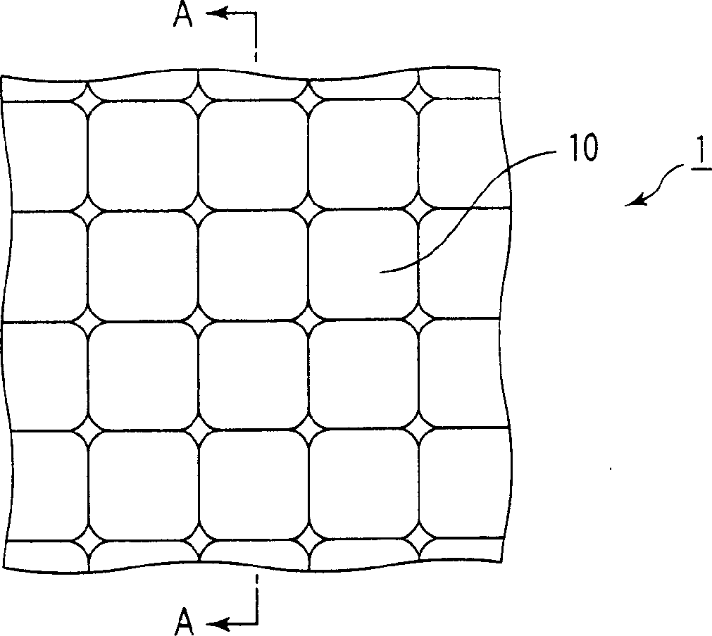
[0036] Figure 2A A plan view of the solid-state imaging device 1 of the first embodiment is shown. also, Figure 2B A sectional view along line A-A of FIG. 1 is shown. First, refer to Figure 2A and Figure 2B Next, the configuration of the solid-state imaging device 1 will be described.

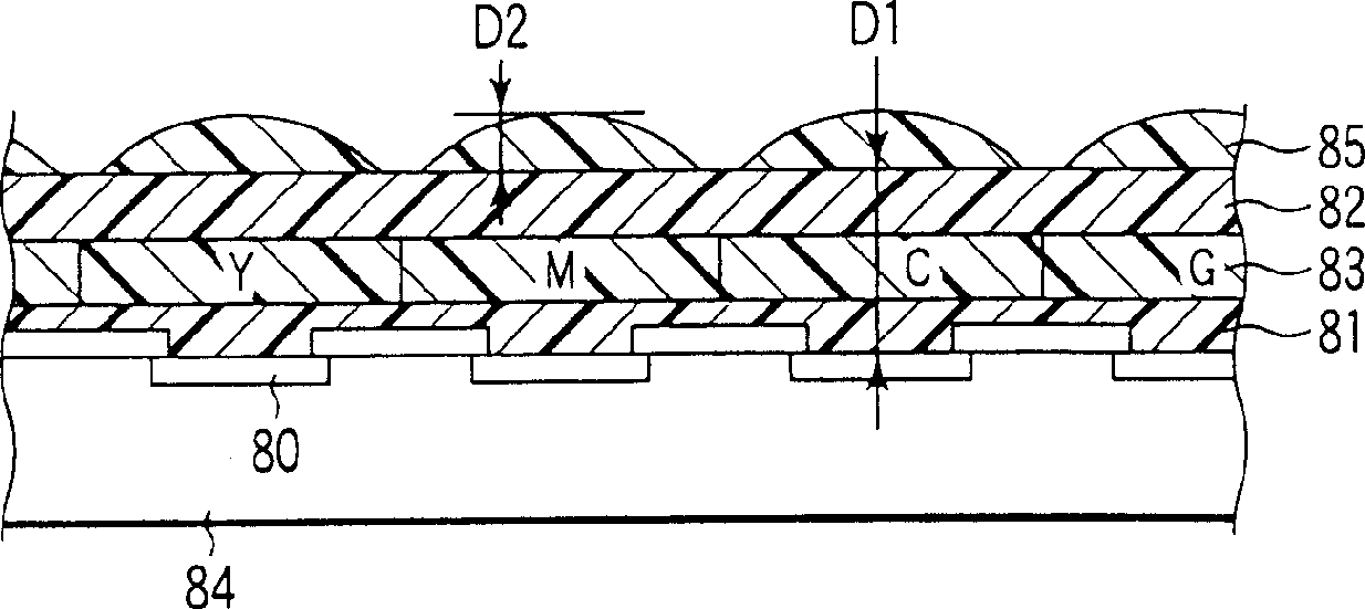
[0037] Such as Figure 2A , Figure 2B As shown, the solid-state imaging device 1 includes a microlens 10 , a semiconductor substrate 11 , a photoelectric conversion element 13 , a light shielding layer 16 , and a planarization layer 15 .

[0038] The semiconductor substrate 11 is a substrate for mounting the photoelectric conversion element 13 and the like. The photoelectric conversion element 13 converts light incident through the microlens 10 into charges. The flattening layer 15 flattens the mounting surface of the microlens 10 .

[0039]The microlens 10 has a hemispherical shape, and has a hemispherical transparent resin upper layer 10 a forming the upper portion of the lens 1...

no. 2 Embodiment approach

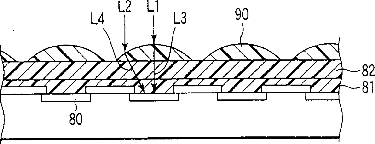
[0072] Figure 4 It is a plan view of the solid-state imaging device 20 of the second embodiment. Figure 5A shows the edge of the solid-state imaging device 20 Figure 4 Sectional view of line A-A. Such as Figure 5A As shown, the solid-state imaging element 20 includes a semiconductor substrate 11 , a photoelectric conversion element 13 , a microlens 10 , a blocking layer 16 , and a planarization layer 15 .

[0073] The microlens 10 has a transparent resin upper layer 10a and a colored lower layer 10b. An infrared absorption function can be imparted to the transparent resin upper layer 10 a and the planarization layer 15 . Generally, an infrared cut filter with a thickness of about 2mm is included in the optical system of a solid-state imaging device for a digital camera or a mobile phone, but by imparting an infrared absorption function to the transparent resin upper layer 10a or the planarizing layer 15, remove the infrared cut filter.

[0074] In addition, if Figu...

no. 3 Embodiment approach

[0113] Figure 9 The edge of the solid-state imaging device 30 of the third embodiment is shown Figure 4 Sectional view of line A-A. First, refer to Figure 9 The configuration of the solid-state imaging device 30 will now be described.

[0114] Such as Figure 9 As shown, the solid-state imaging device 30 includes a microlens 10 , a semiconductor substrate 11 , a photoelectric conversion element 13 , a planarization layer 15 , a blocking layer 16 , and an external resin layer 31 .

[0115] Such as Figure 9 As shown, the thickness T5 of the microlens 10 is the sum of the thickness T1 of the transparent resin upper layer 10a and the thickness T4 of the colored lower layer forming a part of the microlens (the depth to the lens-shaped notch portion of the colored lower layer 10b) (T5 =T1+T4).

[0116] The specific ideal thickness T1 of the transparent resin upper layer 10a, the ideal thickness T2 of the colored lower layer 10b, and the ideal area of ​​the interface betwee...


PUM


Abstract

A solid-state imaging device includes a plurality of two-dimensionally arranged photo diodes and a plurality of microlenses having substantially hemispherical shapes which cover the respective photo diodes. The microlens has a multilayer structure including at least a transparent resin upper layer which forms at least a portion of the substantially hemispherical shape, and a colored lower layer provided on a portion of the transparent resin upper layer which is located above the photo diode, with an interface between the colored lower layer and the transparent resin upper layer having a shape conforming to a surface of the photo diode.

Description

technical field [0001] The present invention relates to a solid-state imaging device typified by a photodetection device such as a C-MOS or a CCD. Background technique [0002] The region (aperture portion) of the photoelectric conversion element on a solid-state imaging element such as a CCD that contributes to photoelectric conversion depends on the size and number of pixels of the solid-state imaging element, and is limited to about 20 to 40% of the total area of ​​the solid-state imaging element. The small aperture directly leads to a decrease in sensitivity, so in order to compensate for this, a light-collecting microlens is generally formed on the photoelectric conversion element. [0003] Recently, however, there is a strong demand for high-resolution solid-state imaging devices with more than 3 million pixels. The aperture ratio of the microlens attached to the high-definition solid-state imaging devices is reduced (that is, the sensitivity is reduced), and noise suc...

Claims


Application Information

Patent Timeline
Patent Type & Authority Applications(China)
IPC IPC(8): G02B3/00G02B5/20H01L27/146H01L31/0216H01L31/0232
CPCH01L27/14621H01L31/02162H01L27/14685H01L27/14627G02B3/0018H01L31/0232G02B3/0056G02B5/201H01L31/02327
Inventor 福吉健藏石松忠北村智史绪方介
Owner TOPPAN PRINTING CO LTD
Why Eureka
Try Eureka