Semiconductor device and method for manufacturing semiconductor device

A technology of semiconductors and amorphous semiconductors, applied in semiconductor/solid-state device manufacturing, semiconductor devices, transistors, etc., can solve the problems of being unsuitable for mass production, long time, etc., to reduce display unevenness, high mobility, and avoid adverse effects Effect

Inactive Publication Date: 2014-12-31
SEMICON ENERGY LAB CO LTD
View PDF1 Cites 0 Cited by
  • Summary
  • Abstract
  • Description
  • Claims
  • Application Information

AI Technical Summary

Problems solved by technology

This means that it takes too much time to manufacture semiconductor devices or thin film transistors, so the method is not suitable for mass production

Method used


Image

  • Semiconductor device and method for manufacturing semiconductor device
  • Semiconductor device and method for manufacturing semiconductor device
  • Semiconductor device and method for manufacturing semiconductor device

Examples


Embodiment 1

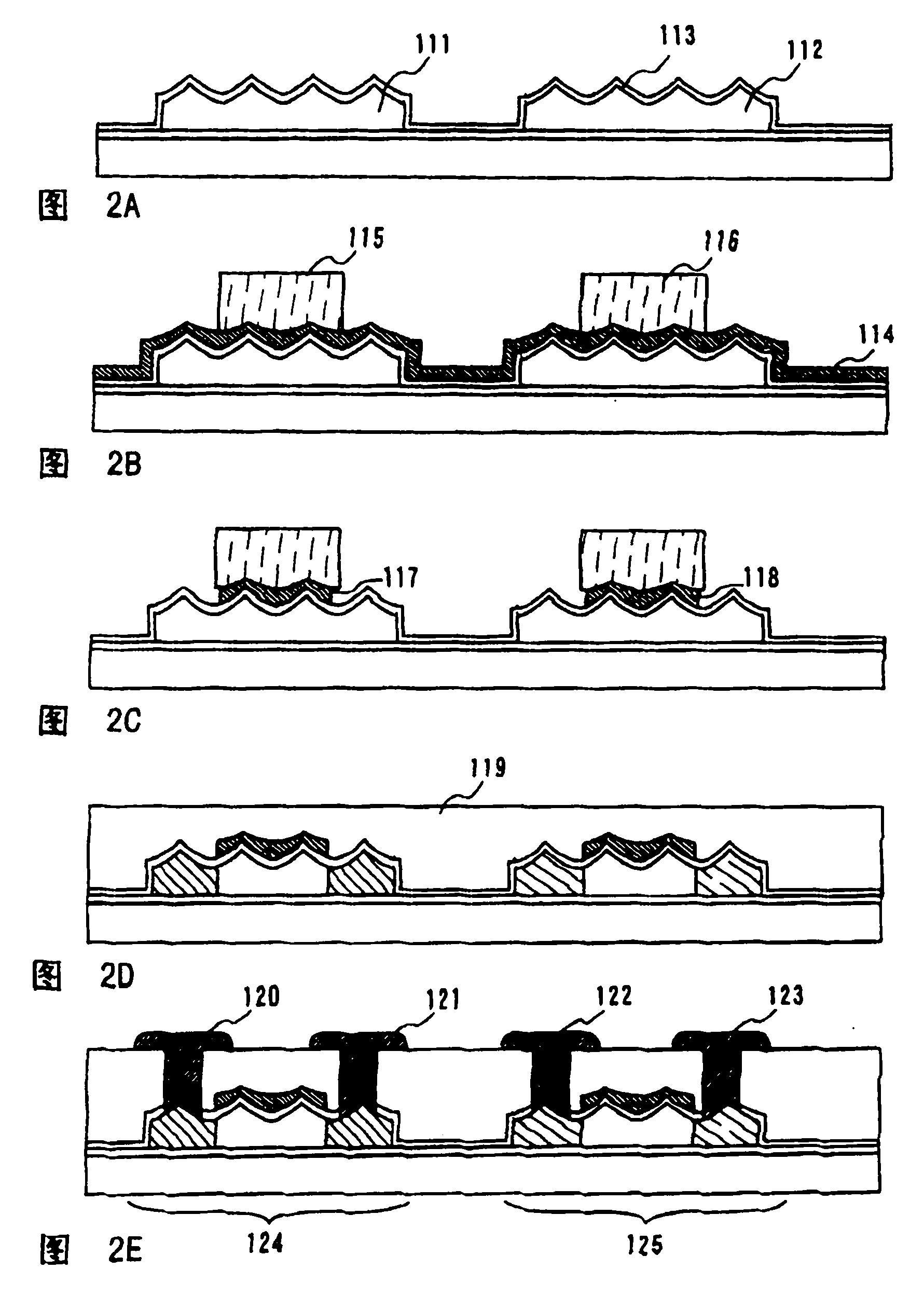
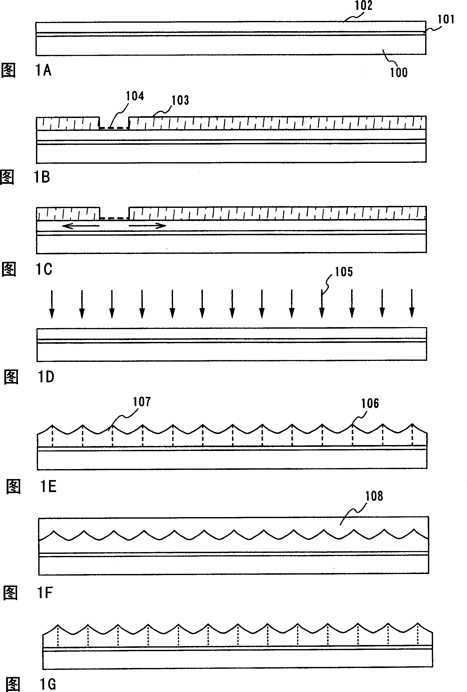
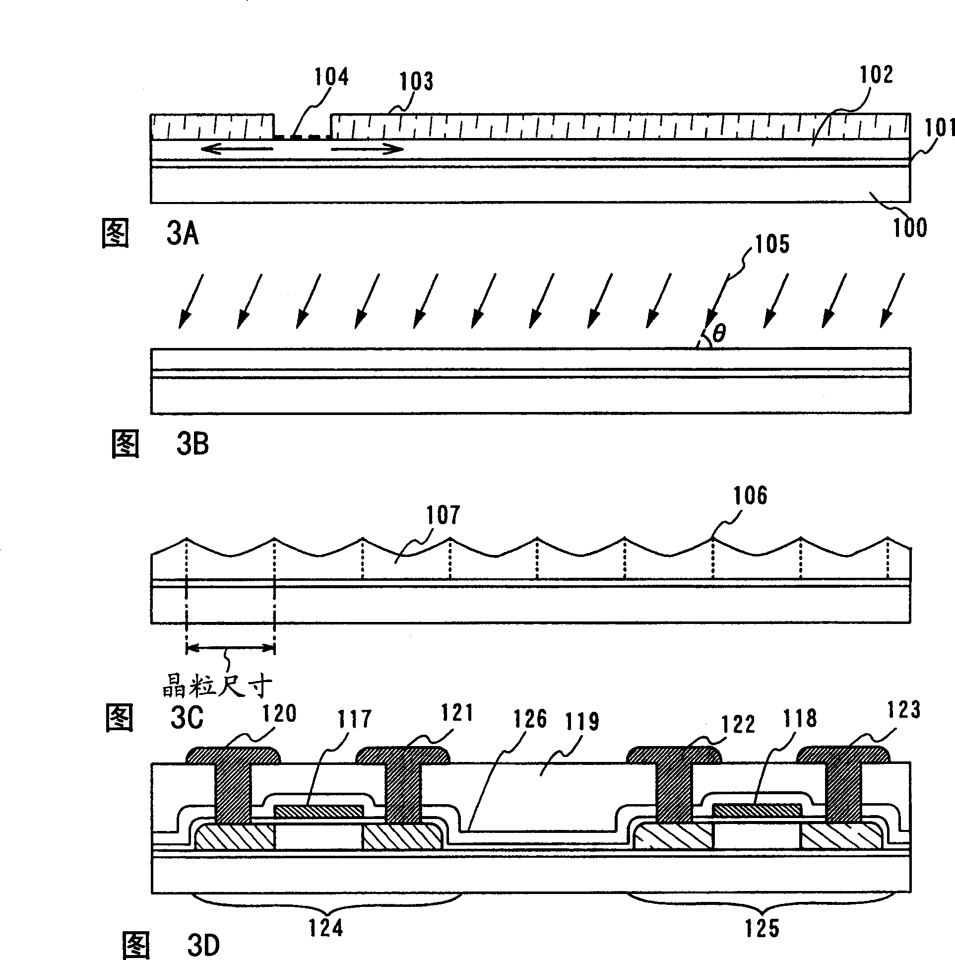
[0230] This example refers to Figures 11A to 11E The principle of ridge formation to maintain order is illustrated.

[0231] Figure 11A Represents the silicon film before being irradiated by pulsed laser light.

[0232] Such as Figure 11B As shown, ridges are formed when irradiating pulsed laser light for the first irradiation. For example, in the case of forming a silicon film to which a metal element promoting crystallization is added and subjected to heat treatment, ridges are formed at positions where grain growth starts from crystal nuclei formed by collision last in the heat treatment. When heat treatment using a metal element is not performed, ridges are formed at random positions.

[0233] Such as Figure 11C As shown, when irradiating pulsed laser light for the second irradiation, scattered light and reflected light (both of which are collectively referred to as diffuse light) increase in laser irradiation due to unevenness generated by ridges on the surface o...


PUM

PropertyMeasurementUnit
sizeaaaaaaaaaa
thicknessaaaaaaaaaa
thicknessaaaaaaaaaa

Abstract

Semiconductor device and method for manufacturing the semiconductor device. An object of the present invention is to provide a crystallization method using a metal element for promoting crystallization to control a crystallographic orientation, wherein a crystalline semiconductor film having an aligned crystallographic orientation is irradiated once with pulsed laser light to form a crystalline semiconductor having small crystal grains film, the ordered spacing of aligned crystal directions in adjacent grains forms small grains in a grid pattern. Still another object of the present invention is to provide a method for producing a crystalline semiconductor film. In view of the above objects, the present invention provides a crystalline semiconductor film having crystal grains formed in a grid pattern in which crystal directions are aligned in adjacent crystal grains, and a thin film transistor having the crystalline semiconductor film. Particularly in the present invention, to form crystal grains having aligned crystal directions among adjacent crystal grains, a metal element for promoting crystallization is selectively added to form a crystalline semiconductor film and thereafter pulsed laser light is preferably irradiated.

Description

technical field [0001] The present invention relates to a semiconductor device having a thin film transistor formed using a crystalline semiconductor film with high crystallinity. The invention also relates to the crystallization process for its manufacture. Background technique [0002] Recently, research on complex semiconductor devices using thin film transistors has progressed. [0003] Especially in semiconductor devices requiring high speed and high functionality, it is necessary to obtain thin film transistors (hereinafter also referred to as TFTs) with high mobility. [0004] In order to enhance the crystallinity of the semiconductor film, crystallization is carried out by adding, constituting, or applying a metal element represented by nickel element (Ni) for promoting crystallization to the semiconductor film, and then heat-treating it to form Crystalline semiconductor film (for example, refer to Patent Document 1). [0005] When a metal element typified by Ni f...

Claims


Application Information

Patent Timeline
Patent Type & Authority Patents(China)
IPC IPC(8): H01L21/20H01L29/786H01L21/336H01L29/04H01L29/76
CPCH01L29/04H01L29/045H01L29/66757H01L29/78696H01L21/02499H01L21/02425H01L21/02686H01L21/02488H01L21/02422H01L21/02532H01L21/0242H01L21/02672H01L21/02595H01L21/02609
Inventor 小路博信下村明久古山将树
Owner SEMICON ENERGY LAB CO LTD
Why Eureka
Try Eureka