Etching device for high precision silicon senser chip

A sensor chip and corrosion device technology, applied in microstructure devices, manufacturing microstructure devices, decorative arts, etc., can solve problems such as easy undercutting, high requirements on process operations, and long processing time, and achieve a high degree of centralized control. , Improve the quality of the reaction, speed up the effect of the reaction process

Inactive Publication Date: 2005-03-30
SHENYANG ACAD OF INSTR SCI
View PDF0 Cites 7 Cited by
  • Summary
  • Abstract
  • Description
  • Claims
  • Application Information

AI Technical Summary

Problems solved by technology

It is mainly manifested in: the working efficiency of the device is low, and the operation of the etching mask (protecting the back circuit, etc.) is complicated; the etching process is full of immersion, so the process operation requires high
At the same time, because the device is based on a chemical test device, its process parameters and various conditions are not easy to be strictly controlled, and the consistency and controllability of silicon wafer etching are relatively poor, especially during the etching process. Undercutting is often prone to occur in corrosive liquids
Low diaphragm thickness control accuracy, low yield, inaccurate final corrosion thickness control of silicon wafers, long processing time and other defects or problems

Method used


Image

  • Etching device for high precision silicon senser chip
  • Etching device for high precision silicon senser chip
  • Etching device for high precision silicon senser chip

Examples


Embodiment Construction

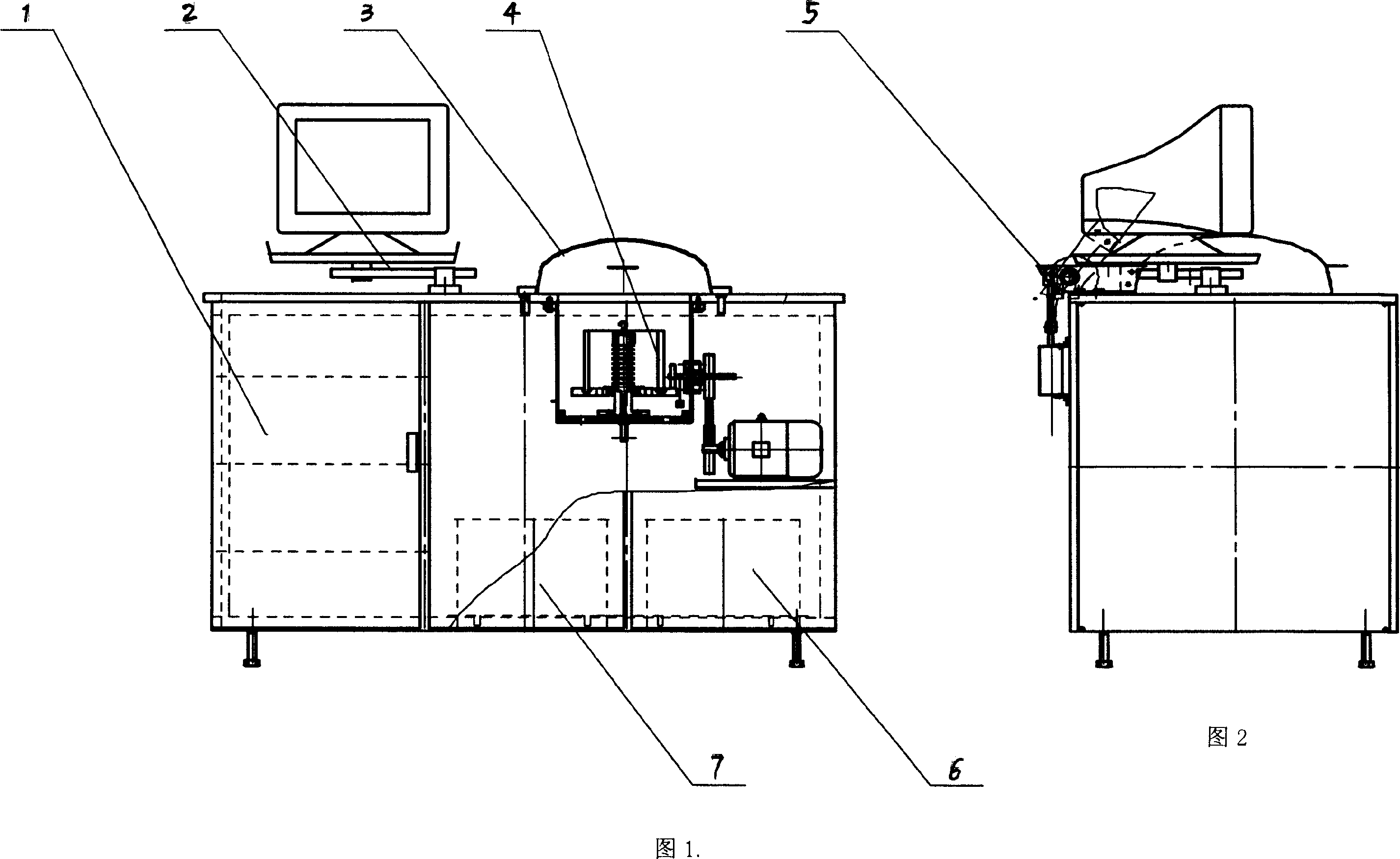
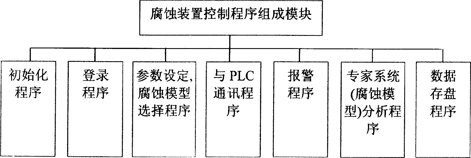
[0020] The composition of each component part of device of the present invention is illustrated in conjunction with accompanying drawing:

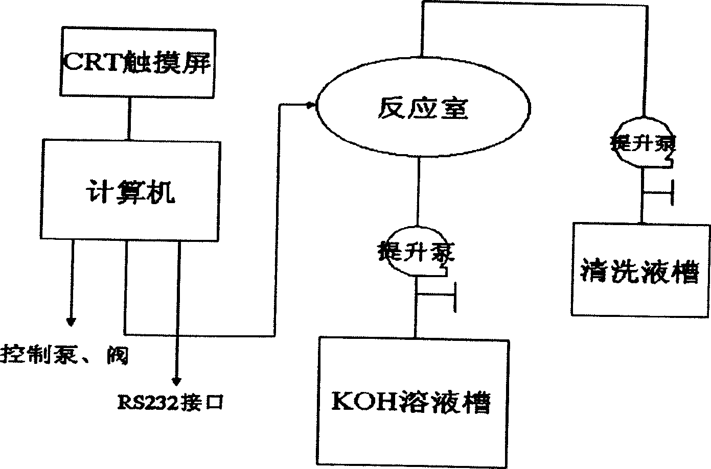
[0021] High-precision silicon sensor chip etching device, see image 3: It includes an industrial computer, a reaction chamber, a KOH liquid storage tank, and a cleaning liquid storage tank. It is characterized in that the computer 2 of the device 1 has a CRT touch screen and an operation control program, and communicates with the control circuit of the electric control cabinet, the reaction chamber 4 and the tube through the communication interface. The valves and pumps on the road are connected; the reaction chamber has a built-in transmission spray mechanism, and its spray pipe is connected to the submerged pump of the KOH liquid storage tank 7 and the cleaning liquid storage tank 6 through the liquid pipeline; the probes for temperature measurement and concentration measurement are respectively Set in the reaction chamber 4.

[0022] ...


PUM

PropertyMeasurementUnit
diameteraaaaaaaaaa

Abstract

The equipment includes industrial control computer, electric appliance control cabinet, reaction chamber, KOH stock solution pot and cleaning liquid stock solution pot. The computer including CRT touch screen and job control program through communication interface is connected to control circuit of electric control cabinet, reaction chamber as well as valves and pumps on pipe. Transmission sprinkle mechanism is built in reaction chamber, and sprinkle tube through liquid pipe is connected to immersible pumps in KOH stock solution pot and cleaning liquid stock solution pot. Probes for detecting temp and density of KOH are setup in the reaction chamber. Computer control is adopted in the equipment. Thus simple operation and production in scale (six wafers in four inches in one time) are realized. Sprinkle technique makes etching process in better environment of washing out and reacting. The suitable wafer to be etched includes all wafers with diameters smaller than 110mm.

Description

[0001] Field [0002] The invention relates to an etching device for a silicon chip used in a wet chemical etching process for a silicon sensor. Background technique [0003] The silicon sensor etching device is one of the key equipment in the batch silicon sensitive diaphragm preparation process in the sensor MEMS micromachining manufacturing technology. Its mechanism is to conduct directional etching on the surface of silicon wafers through wet chemical etching process to achieve the purpose of mass production of silicon sensor sensitive diaphragms. [0004] There are no domestic and foreign reports related to the "high-precision silicon wafer etching device", but the simple device and etching process technology for forming the required silicon diaphragm by means of wet chemical etching are well known both at home and abroad. There are many articles on it. In the past, some simple and related silicon wafer etching devices were prepared for the needs of scientific research,...

Claims


Application Information

Patent Timeline
Patent Type & Authority Applications(China)
IPC IPC(8): B81C1/00C23F1/32H01L21/3063
Inventor 刘沁匡石张纯棣陈信琦
Owner SHENYANG ACAD OF INSTR SCI
Why Eureka
Try Eureka