Auxiliary grid hot wire chemical vapor deposition process for preparing nano-diamond thin film

A technology of nano-diamond and vapor deposition method, which is applied in the field of preparing nano-diamond film, which can solve the problems of destroying the smooth surface of the substrate and affecting the flatness and smoothness of the film.

Active Publication Date: 2005-04-06
SHANGHAI JIAO TONG UNIV +1
View PDF0 Cites 12 Cited by
  • Summary
  • Abstract
  • Description
  • Claims
  • Application Information

AI Technical Summary

Problems solved by technology

Using the above method, the substrate must be roughened with 0.5 μm diamond micropowder grinding before deposition to enhance the nucleation density of the diamond film, which will affect the flatness and smoothness of the film. In this case, it is very difficult It is difficult to deposit a very smooth nano-diamond film on the surface of the substrate, and the above-mentioned method is based on the silico...

Method used


Image

  • Auxiliary grid hot wire chemical vapor deposition process for preparing nano-diamond thin film
  • Auxiliary grid hot wire chemical vapor deposition process for preparing nano-diamond thin film
  • Auxiliary grid hot wire chemical vapor deposition process for preparing nano-diamond thin film

Examples


Embodiment Construction

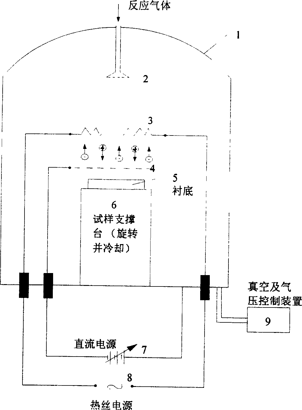
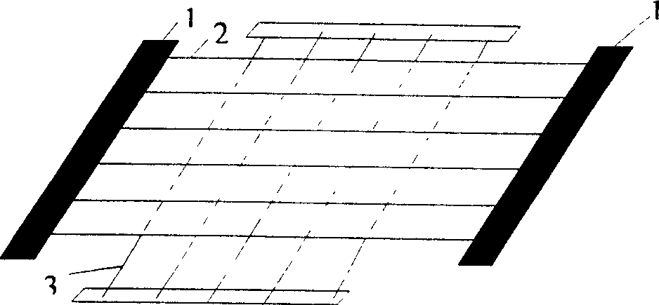
[0015] In order to better deal with the technical solution of the present invention, the planar substrate is taken as an example below, combined with the auxiliary hot-wire CVD device and coating detection results for further description. figure 1 is the schematic diagram of the auxiliary grid hot wire CVD device, in which 1 is the reaction chamber, 2 is the reaction gas inlet, 3 is the hot wire (a group of Czochralski parallel hot wires), 4 is the auxiliary grid (a group of parallel graphite strips), and the thermal The plane where the wire is located is parallel to the plane where the grid is located, but if figure 2 As shown, the direction of the hot wire 2 is perpendicular to the direction of the grid strip 3, 5 is the sample (planar substrate), 6 is the sample support platform, which can rotate and cool, and 7 is the DC adjustable power supply ( The hot wire is connected to the positive pole, the grid is connected to the negative pole), 8 is the hot wire power supply, wh...


PUM


Abstract

One kind plates covers the area of technology the preparation nanometer diamond thin film auxiliary electronics grid hot filament chemistry gas phase sedimentation, in in the hot filament CVD deposition diamond thin film foundation, increases a kind of auxiliary electronics grid, the auxiliary electronics grid in the hot filament deposition initial period, deposits in advance a diamond thin film, then adds on the direct current bias between the electronics grid and the hot filament, the electronics grid for negative, the electronics grid surface diamond thin film is the launch electron forms the direct current electric discharge, cation will shell the electronics grid, the diamond atom and the atomic group which will shell down splashes down to the substrate on, will become the diamond shape nucleus and the growth driving point, The sputtering the diamond high density shape nucleus and quadratic form the nucleus played the key role to the substrate on, the substrate surface deposition obtained the nanometer diamond thin film. The invention can reach to the limit the high shape nuclear density, simultaneously has the very high two speeds in the growth process, can grow obtains a nanometer level the diamond thin film, after the deposition the thin film does not need to grind polishes can achieve a higher smooth finish, satisfies the operation requirements.

Description

technical field [0001] The invention relates to a method for preparing a nano-diamond film, in particular to an auxiliary grid hot-wire chemical vapor deposition method for preparing a nano-diamond film, which is used in the technical field of plating. Background technique [0002] With the development and maturity of CVD diamond film deposition technology, nano-diamond film coating technology has rapidly become a new hotspot in the field of CVD diamond film research. Nano-diamond film grains are very small, ranging from several to tens of nanometers, two orders of magnitude smaller than conventional diamond films, the surface is extremely smooth, the surface roughness can be below Ra100nm, and the friction coefficient of the film is very small, only 0.03 ~0.06, much lower than 0.2~1.1 of conventional diamond film. The emergence of nano-diamond films makes it possible to directly obtain diamond films with smooth surfaces on substrate materials. More importantly, the deposit...

Claims


Application Information

Patent Timeline
IPC IPC(8): C23C16/27C23C16/503
Inventor 孙方宏张志明沈荷生郭松寿
Owner SHANGHAI JIAO TONG UNIV
Why Eureka
Try Eureka