Semiconductor storage device
A technology for memory devices and semiconductors, which is applied in the field of eliminating through current generated during operation and reducing peak current, and can solve the problems of semiconductor memory device failure, source potential reduction, etc., to eliminate through current, reduce peak current, and achieve high-speed characteristics. Effect
- Summary
- Abstract
- Description
- Claims
- Application Information
AI Technical Summary
Problems solved by technology
Method used
Image
Examples
no. 1 example
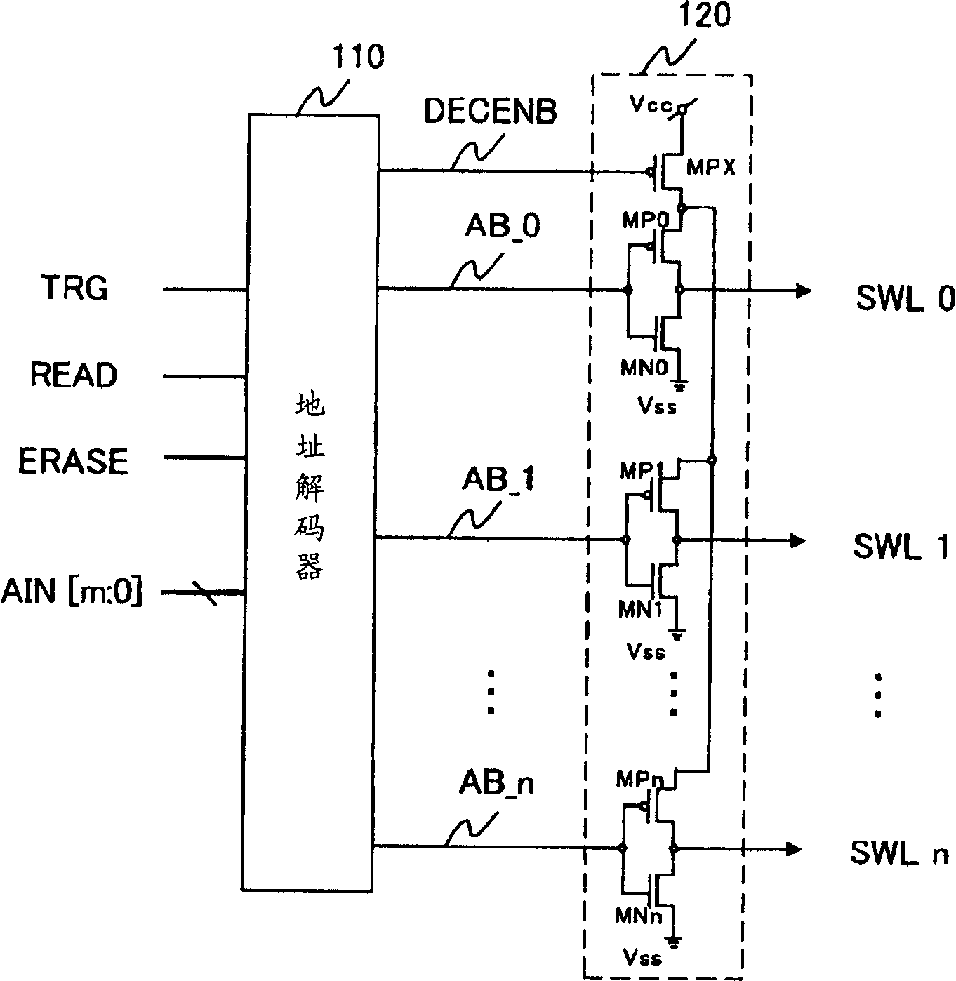
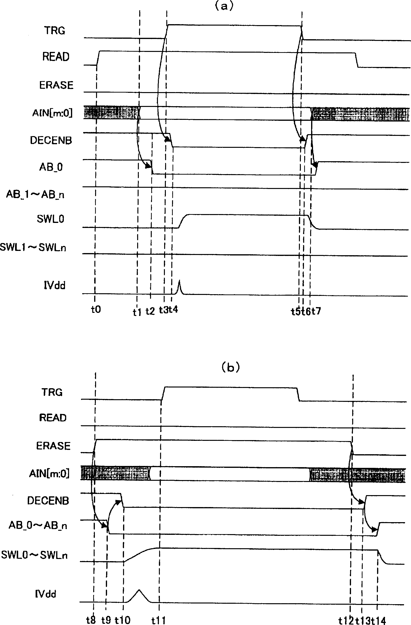
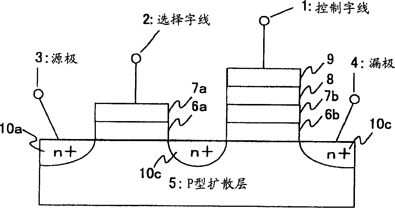
[0056] figure 1 is a circuit diagram showing the structure of the word line driving circuit in the semiconductor memory device according to the first embodiment. In this embodiment, transistors having both functions of adjusting timing and limiting current in order to prevent shoot-through current and reduce peak current are provided separately from word line driving unit circuits for individually driving respective word lines. The semiconductor element driven by the word line driving unit circuit of the present invention is, for example image 3 EEPROM shown. Since the structure of the EEPROM has been described above, its explanation is omitted here. The word line driven by the word line driving unit circuit is image 3 "Select Word Line" indicated by reference numeral 2 in . It is not necessary to specifically boost the select word line 2 differently from the control word line 1 .
[0057] figure 1Among them, a TRG signal, a READ signal, an ERASE signal and an address ...
no. 2 example
[0073] see Figure 4 and 5 , the operation and structure of the word line driver circuit in the semiconductor device of this embodiment will be described below. Figure 4 in, with figure 1 Parts of the circuits shown that have the same function are denoted and described with the same reference numerals.
[0074] The basic structure and the figure 1 The basic structure of the circuit shown is the same. But when Figure 4 in, with figure 1 The circuit shown differs in that an Nch transistor MNX for current limitation is also provided on the ground potential side. Then, the potential change becomes slow until the word line potential returns to the ground potential Vss, so that the peak current can be reduced more. That is, in Figure 4 Among them, one or more Nch transistors (MNX) are respectively provided on the ground terminal side of the Nch transistors (MN0˜MNn) of the plurality of word line driving unit circuits.
[0075] The current supply amount of the Nch tran...
no. 3 example
[0080] This embodiment is different from the first and second embodiments in that the operation of each transistor itself forming a word line driving unit circuit for driving a word line can be independently controlled. Two transistors having different current supply amounts are provided as transistors provided on the source potential side (power supply side). These transistors switch appropriately to prevent shoot-through current and reduce peak current.
[0081] Such as Figure 6 As shown, a word line driving unit circuit in the word line driving circuit 120 includes: two Pch transistors (MPR0, MPE0, etc.) and one Nch transistor (MN0, etc.) with different current supply levels, and their drains are connected to Together. Therefore, the word line driving unit circuit of this embodiment is a CMOS push-pull driver. Independent control signals (RA-0, EA-0, EN-0, etc.) are input to the gates of the three transistors respectively. In this way, the operation of each transistor ...
PUM
 Abstract
Description
Claims
Application Information
 - R&D
- Intellectual Property
- Life Sciences
- Materials
- Tech Scout
- Unparalleled Data Quality
- Higher Quality Content
- 60% Fewer Hallucinations
Browse by: Latest US Patents, China's latest patents, Technical Efficacy Thesaurus, Application Domain, Technology Topic, Popular Technical Reports.
© 2025 PatSnap. All rights reserved.Legal|Privacy policy|Modern Slavery Act Transparency Statement|Sitemap|About US| Contact US: help@patsnap.com


