Matrix addressing vertical cavity surface emitting laser array device

A technology of vertical cavity surface emission and laser array, which is applied in the direction of laser components, lasers, semiconductor lasers, etc., can solve the problems of high process requirements, low reliability and repeatability, and difficult process, and achieve multi-addressing, Avoid the drift of the reflection peak wavelength and the effect of high reflectivity

Inactive Publication Date: 2005-06-01
INST OF SEMICONDUCTORS - CHINESE ACAD OF SCI
View PDF0 Cites 12 Cited by
  • Summary
  • Abstract
  • Description
  • Claims
  • Application Information

AI Technical Summary

Problems solved by technology

These current production methods have a significant disadvantage, that is, they have relatively high re

Method used


Image

  • Matrix addressing vertical cavity surface emitting laser array device
  • Matrix addressing vertical cavity surface emitting laser array device
  • Matrix addressing vertical cavity surface emitting laser array device

Examples


Example Embodiment

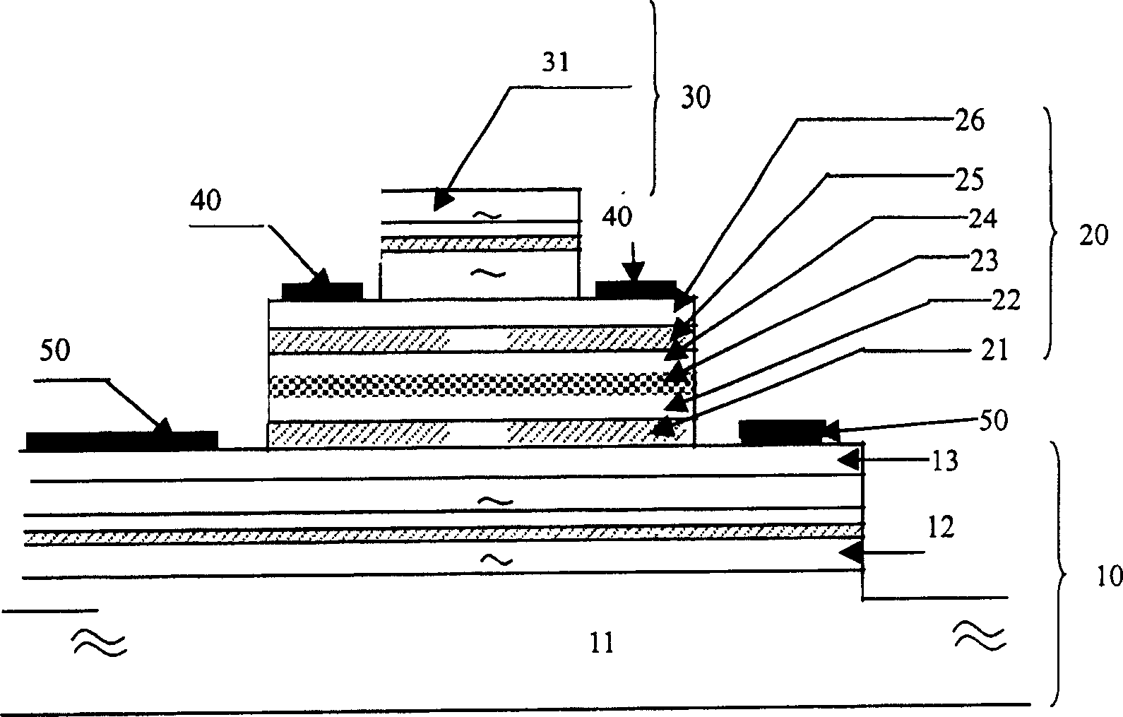
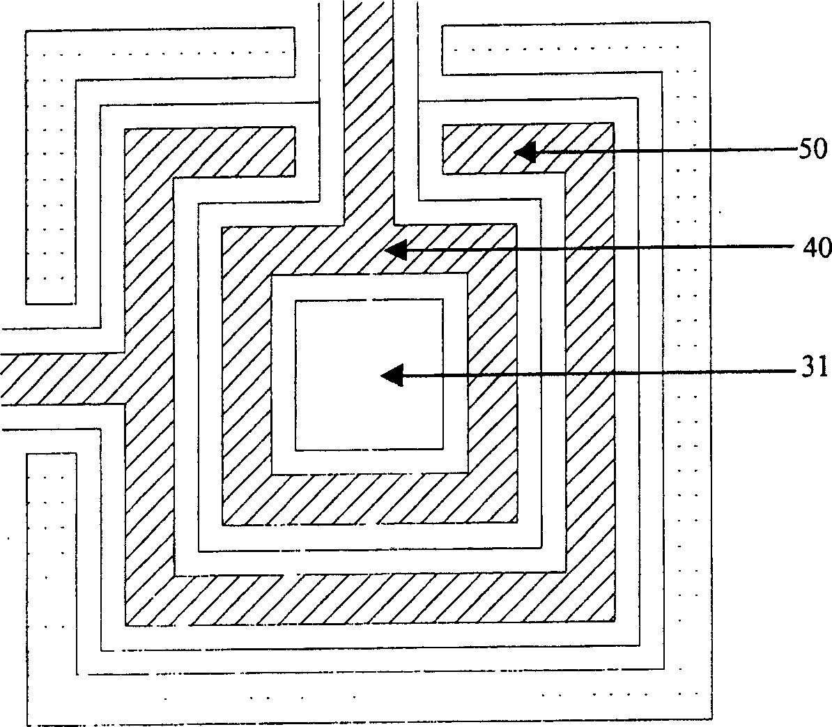
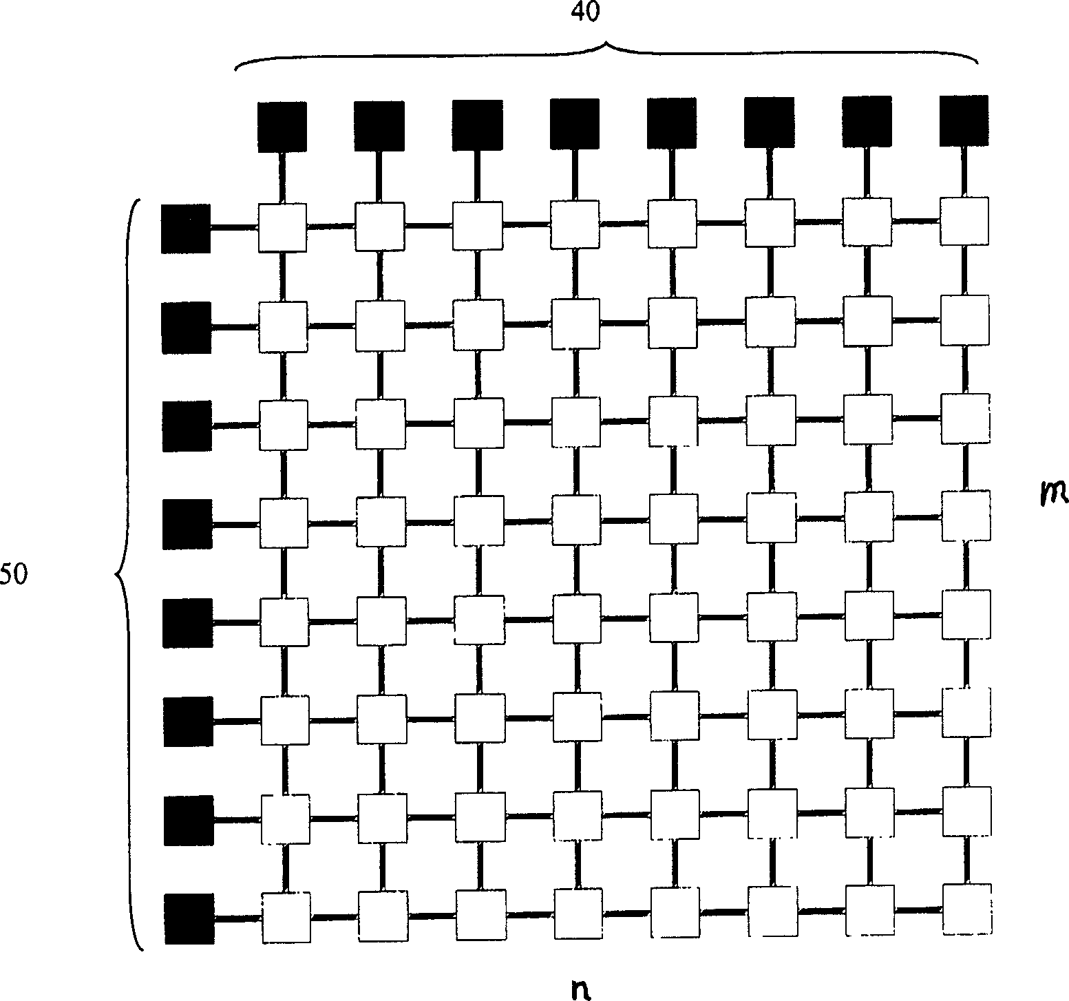
[0043] This embodiment includes a total of 8 rows and 8 columns, a total of 8 × 8 vertical cavity surface emitting laser units (see attached image 3 );

[0044] Combine below figure 1 with figure 2 , Describe the basic structure of the embodiment of the present invention.

[0045] Each vertical cavity surface emitting laser unit includes three stages with successively decreasing sizes: a bottom reflection mirror stage 10, an optical cavity stage 20, and a top reflection mirror stage 30, as well as a p-electrode 40 and an n-electrode 50;

[0046] The bottom reflector stage 10 includes:

[0047] Half of the insulating substrate 11;

[0048] -Gallium arsenide / alumina lower Bragg reflector 12;

[0049] An n-type heavily doped gallium arsenide conductive layer 13;

[0050] The optical cavity stage 20 includes:

[0051] An n-type doped aluminum gallium arsenide layer 21;

[0052] An undoped gallium arsenide lower confinement layer 22;

[0053] An undoped gallium arsenide / aluminum gall...


PUM


Abstract

The matrix addressed vertical cavity emitting laser array device includes mXn vertical cavity emitting laser units. Each of the vertical cavity emitting laser units includes three mesas, including bottom reflector mesa, laser cavity mesan and top reflector mesa, of successively decrementing sizes as well as p electrode and n electrode. The laser cavity mesan is made on the bottom reflector mesa, and the top reflector mesan is made on the laser cavity mesa. The p electrode is made on the p-type re-doped conducting layer and around the top reflector mesa, and the p electrodes of each row of the vertical cavity emitting laser units are connected together. The n electrode is made on the n-type re-doped conducting layer and around the laser cavity mesa, and the n electrodes of each line of the vertical cavity emitting laser units are connected together.

Description

Technical field: [0001] The invention relates to an optoelectronic integrated device, in particular to a novel matrix addressing vertical cavity surface emitting laser array device. Background technique: [0002] Two-dimensional array parallel light technology has broad application prospects. When two-dimensional parallel beams are used to process two-dimensional image information, it does not need to be transformed into sequential signals, which can increase the processing speed; can develop ultra-wideband optical fiber communication; can realize the optical interconnection of VLSI; it may become a future computer parallel processing and Key technologies and devices in space optics. Edge-emitting lasers (including FP and DFB type edge-emitting lasers) cannot realize monolithically integrated two-dimensional arrays, while surface-emitting lasers emit light upward perpendicular to the substrate, and it is possible to realize monolithically integrated two-dimensional arrays. ...

Claims


Application Information

Patent Timeline
IPC IPC(8): H01S5/183H01S5/42
Inventor 刘志宏王圩
Owner INST OF SEMICONDUCTORS - CHINESE ACAD OF SCI
Why Eureka
Try Eureka