Bipolar transistor
一种双极晶体管、晶体材料的技术,应用在晶体管、半导体器件、半导体/固态器件制造等方向,能够解决高频区功率增益低等问题,达到低功耗的效果
- Summary
- Abstract
- Description
- Claims
- Application Information
AI Technical Summary
Problems solved by technology
Method used
Image
Examples
no. 1 approach
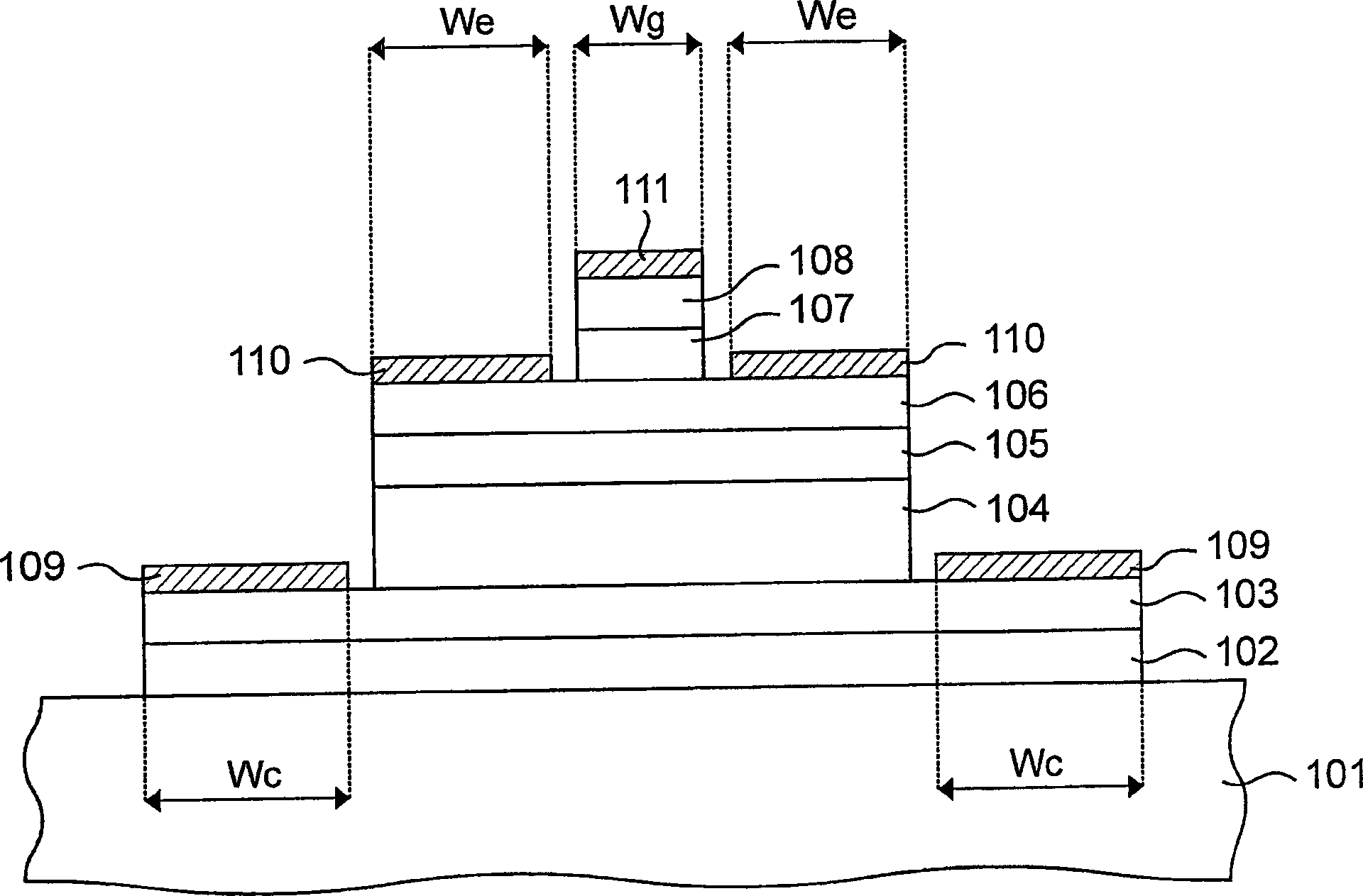
[0091] Figure 7 A cross-sectional structure diagram of a device to which the first embodiment of the present invention is applied is shown.
[0092] The device has an n-GaN sub-collector layer (layer thickness: 100nm, N d =5×10 18 cm -3 ) 703, the n-In formed in the center region of the upper surface of the sub-collector layer 703 X Ga 1-X N collector layer (layer thickness: 500nm, composition ratio (composition ratio) X=0→0.2, N d =1×10 16 cm -3 ) 704, p-In as the second conductivity type carrier retention layer 0.2 Ga 0.8 N base layer (layer thickness: 25nm, N a =5×10 19 cm -3 ) 705, n-GaN emitter layer (layer thickness: 80nm, N d =5×10 18 cm -3 ) 706 and the p-Al formed in the center region of the upper surface of the emitter layer 706 0.2 Ga 0.8 N gate layer (layer thickness: 50nm, N a =5×10 18 cm -3 )707. n-In X Ga 1-X The In crystal mixing ratio X of the N collector layer 704 is graded such that X=0 on the sub-collector layer side and X=0.2 on the ...
no. 2 approach
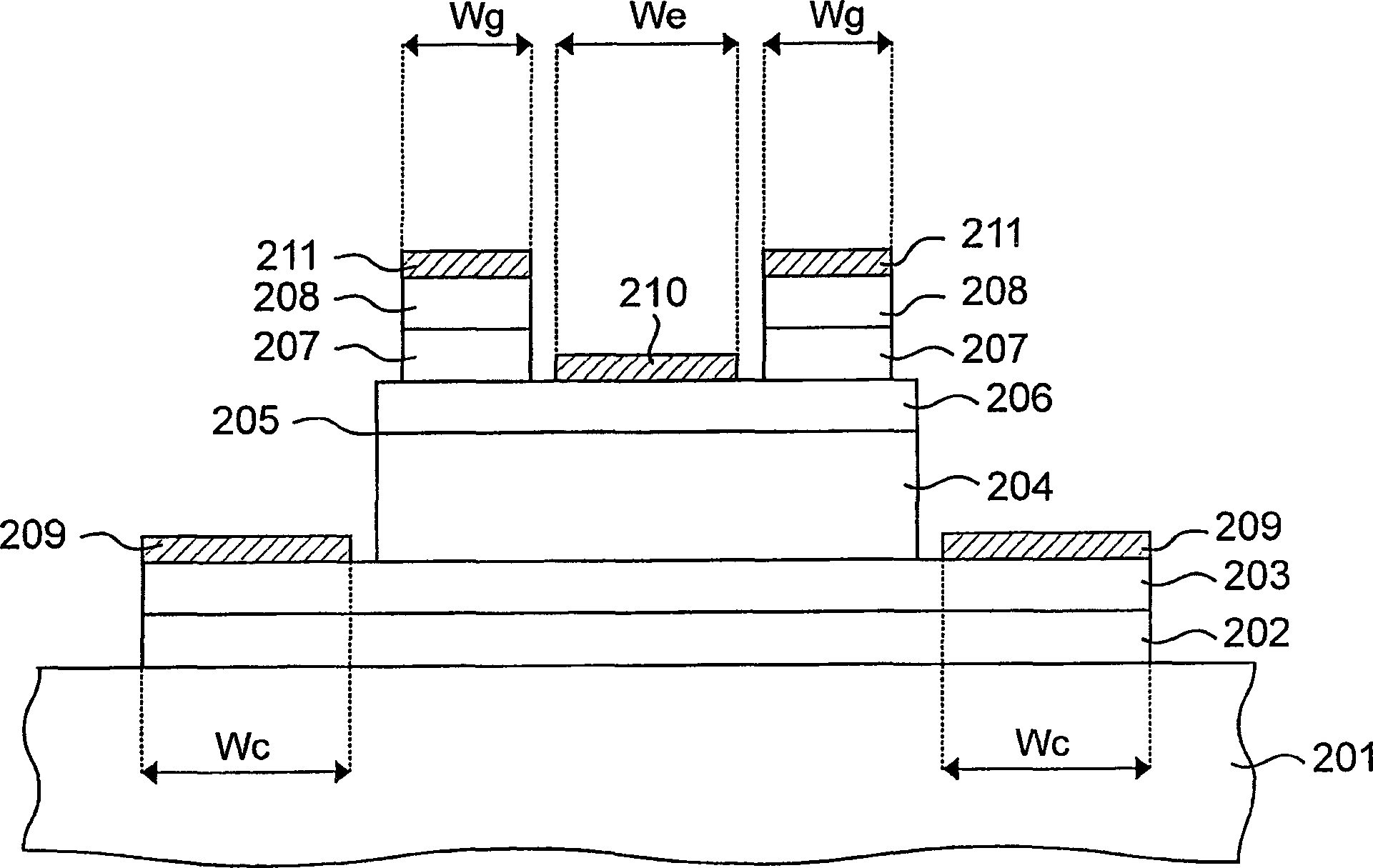
[0106] Figure 10 A sectional structural view of a device to which the second embodiment of the present invention is applied is shown.
[0107] The device has an n-GaN sub-collector layer (layer thickness: 100nm, N d =5×10 18 cm -3 ) 1003, the n-In formed in the center region of the upper surface of the sub-collector layer 1003 X Ga 1-X N collector layer (layer thickness: 500nm, In composition ratio X=0→0.2, N d =1×10 16 cm -3 ) 1004, n-GaN emitter layer (layer thickness: 80nm, N d =5×10 18 cm -3 ) 1006 and the p-Al formed in the center region of the upper surface of the emitter layer 1006 0.2 Ga 0.8 N gate layer (layer thickness: 50nm, N a =5×10 18 cm -3 )1007. n-In X Ga 1-X The In crystal mixing ratio X of the N collector layer 1004 is graded such that X=0 on the sub-collector layer side and X=0.2 on the emitter layer side.
[0108] A collector electrode 1009, an emitter electrode 1010, and a gate electrode 1011 are formed similarly to the first embodiment....
no. 3 approach
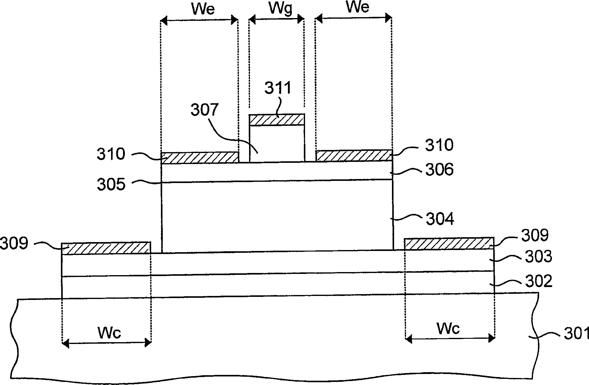
[0118] Figure 12 A cross-sectional structural diagram of a device to which the third embodiment of the present invention is applied is shown.
[0119] The device has an n-GaN sub-collector layer (layer thickness: 100nm, N d =5×10 18 cm -3 ) 1203, the n-In formed in the central region of the upper surface of the sub-collector layer 1203 X Ga 1-X N collector layer (layer thickness: 500nm, In composition ratio X=0→0.2, N d =1×10 16 cm -3 ) 1204, n-GaN emitter layer (layer thickness: 80nm, N d =5×10 18 cm -3 ) 1206 and the Al formed in the central region of the upper surface of the emitter layer 1206 X Ga 1-X N gate layer (layer thickness: 25nm, Al composition ratio X=0.1→0.3, undoped) 1207 . n-In X Ga 1-X The In crystal mixing ratio X of the N collector layer 1204 is graded so that X=0 on the sub-collector layer side and X=0.2 on the emitter layer side. And, Al X Ga 1-X The Al crystal mixing ratio X of the N gate layer 1207 is graded so that X=0.1 on the emitter...
PUM
 Abstract
Description
Claims
Application Information


