

Exposure device
A technology of exposure device and exposure system, which is applied in the direction of photolithography exposure device, microlithography exposure equipment, electrical components, etc., can solve the problems of unreasonable structure, error, and low positioning accuracy, and achieve the reduction of deformation and vibration, Improved stability and reduced vibration
- Summary
- Abstract
- Description
- Claims
- Application Information
AI Technical Summary
Problems solved by technology
Method used
Image

Examples
Embodiment Construction
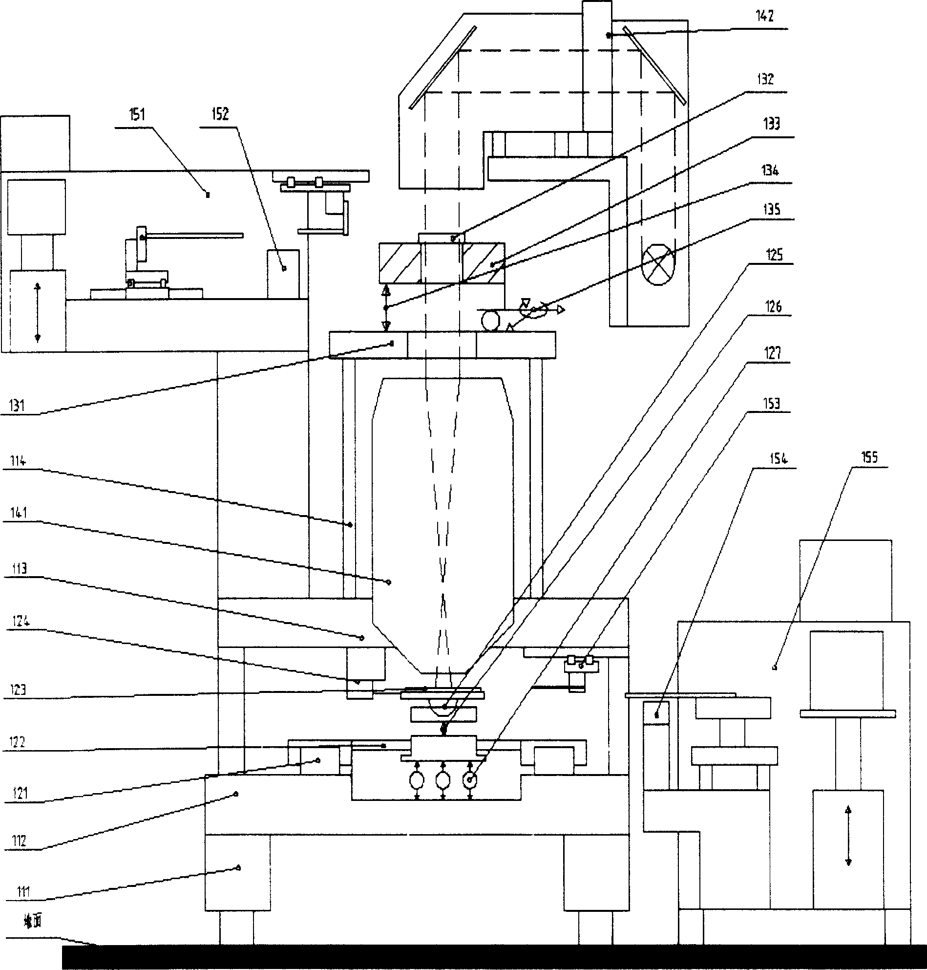
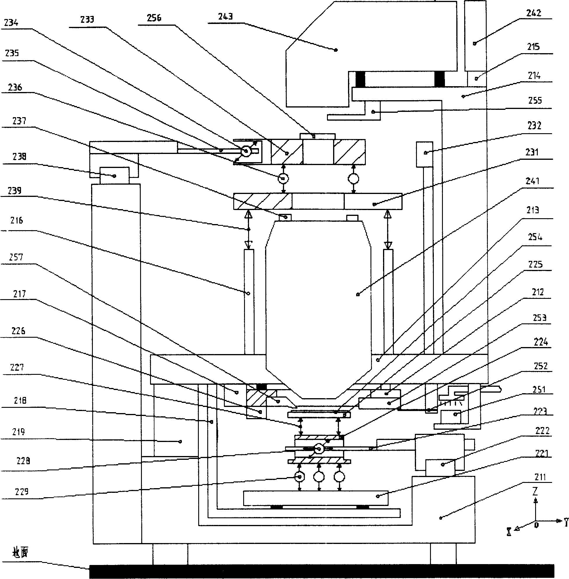
[0058] figure 2 and image 3 It is a structural schematic diagram of an embodiment of an exposure device according to the present invention. As shown in the figure: the exposure device is composed of the whole machine frame, vibration reduction system, precision motion system, precise real-time measurement system, alignment system, precision exposure system and drive motor.
[0059] Among them, the overall frame includes: external frame 211, measurement substrate 212, main substrate 213, lighting support 214, mask table support 216, hanging frame 218; using active shock absorber 219, we will place it on the active shock absorber 219 The frames are called inner frames and the rest are outer frames. The drive motors 222, 223, 235, 238 are fixed on the outer frame 211, and the precision motion system, precision real-time measurement system, alignment system, and precision exposure system are located on the inner frame.
[0060] The damping system includes active dampers 215, ...
PUM
 Abstract
Description
Claims
Application Information