Semiconductor device

A semiconductor and conductive technology, which is applied in the direction of semiconductor devices, connection grounds, electrical components, etc., can solve problems such as difficult control of withstand voltage, and achieve the effect of easy control

Inactive Publication Date: 2005-08-31
SANYO ELECTRIC CO LTD
View PDF2 Cites 5 Cited by
  • Summary
  • Abstract
  • Description
  • Claims
  • Application Information

AI Technical Summary

Problems solved by technology

However, it is very difficult to obtain the specified forward voltage VF characteristics and leakage current IR characteristics, and to ensure the specified withstand voltage. In fact, it is necessary to sacrifice some of them for design

Method used


Image

  • Semiconductor device
  • Semiconductor device
  • Semiconductor device

Examples


Embodiment Construction

[0050] refer to Figure 1 ~ Figure 3 Embodiments of the present invention will be described in detail.

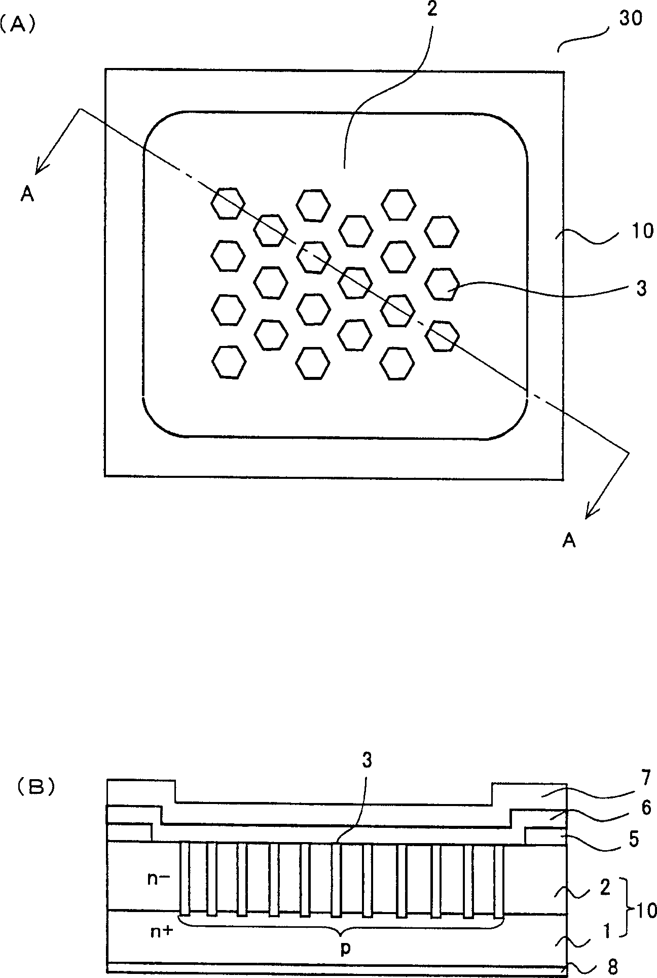
[0051] figure 1 Shows the Schottky barrier diode of the present invention. figure 1 (A) is a floor plan, figure 1 (B) is figure 1 (A) A-A line profile. in addition, figure 1 In (A), the Schottky metal layer and the anode electrode on the substrate surface are omitted.

[0052] The Schottky barrier diode of the present invention is composed of a conductivity type semiconductor substrate 1 , a conductivity type semiconductor layer 2 , a reverse conductivity type semiconductor region 3 and a Schottky metal layer 6 .

[0053] The substrate 10 is a substrate in which an n − -type semiconductor layer 2 is laminated on an n + -type semiconductor substrate 1 by epitaxial growth or the like.

[0054]The reverse conductivity type semiconductor region 3 is a p-type semiconductor region provided on the n-type semiconductor layer 2 . For example, a channel is provided on th...


PUM


Abstract

The conventional Schottky barrier diode has a problem that the increase in leak current is evitable for realizing low VF due to the VF and IR characteristics of the Schottky barrier diode are in a trade-off relation. In the semiconductor device of this invention, pillar shaped p type semiconductor regions that reach an n+ type semiconductor substrate are provided in an n- type semiconductor layer, so that when a reverse voltage is applied, the part of the n- type semiconductor layer between the p type semiconductor regions is filled completely by a depletion layer expanding from the p type semiconductor region and in the horizontal direction of the substrate. In other words, the leakage of the leak current generated at the Schottky junction interface to the cathode side can be suppressed. Moreover, since the impurity concentration in the n- type semiconductor layer can be increased to the extent that the depletion layer expanding from the adjacent p type semiconductor regions can still pinch off, the low VF can be realized, and a predetermined breakdown strength can be secured as long as the depletion layer can pinch off.

Description

technical field [0001] The present invention relates to a semiconductor device, and more particularly, to a semiconductor device that achieves a reduction in the forward voltage VF of a Schottky barrier diode and a reduction in a reverse current IR, and secures a predetermined withstand voltage. Background technique [0002] A Schottky junction formed using a silicon semiconductor substrate and a metal layer has a rectifying effect through its potential barrier, so it is generally an excellent component as a Schottky barrier diode. [0003] Figure 4 Indicates an existing Schottky barrier diode. [0004] Such as Figure 4 (A) An n-type semiconductor layer 32 is laminated on an n+-type semiconductor substrate 31, and a Schottky metal layer 36 forming a Schottky junction with the surface thereof is provided. The metal layer is, for example, Ti. In addition, an Al layer serving as the anode electrode 37 is provided to cover the entire surface of the metal layer. A guard ring...

Claims


Application Information

Patent Timeline
Patent Type & Authority Applications(China)
IPC IPC(8): H01L29/872H01L29/47H01L29/861H01L31/062
CPCH01L29/861H01L29/872H01R4/66H02G13/40
Inventor 冈田哲也斋藤洋明
Owner SANYO ELECTRIC CO LTD
Why Eureka
Try Eureka