Supercharge Your Innovation With Domain-Expert AI Agents!

Method for forming polycrystalline silicon-germanium layer

A technology of polycrystalline silicon germanium and dielectric layer, which is applied in the direction of electrical components, semiconductor/solid-state device manufacturing, circuits, etc., can solve the problems of polycrystalline silicon germanium layer surface roughness, poor process variables, cost increase, etc., to solve gate depletion effect, Simple process, low cost effect

Active Publication Date: 2005-09-07
UNITED MICROELECTRONICS CORP
View PDF0 Cites 0 Cited by
  • Summary
  • Abstract
  • Description
  • Claims
  • Application Information

AI Technical Summary

Problems solved by technology

However, additionally forming a polysilicon seed layer on the oxide layer and then forming a polysilicon germanium layer will affect the electrical properties of the polysilicon germanium gate field effect transistor.
In addition, forming an additional polysilicon seed layer means an increase in cost, additional process variables and poor electrical properties. Therefore, there are still shortcomings to be overcome in the method of using a polysilicon seed layer to solve the surface roughness of the polysilicon germanium layer. This is the principle purpose of the invention

Method used


Image

  • Method for forming polycrystalline silicon-germanium layer
  • Method for forming polycrystalline silicon-germanium layer
  • Method for forming polycrystalline silicon-germanium layer

Examples


Embodiment Construction

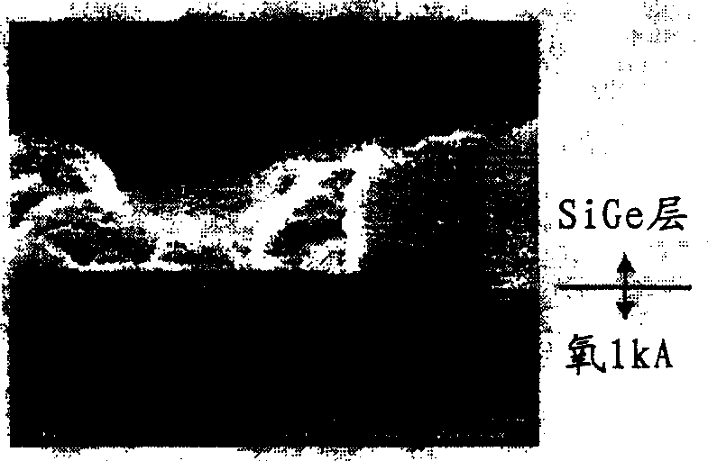
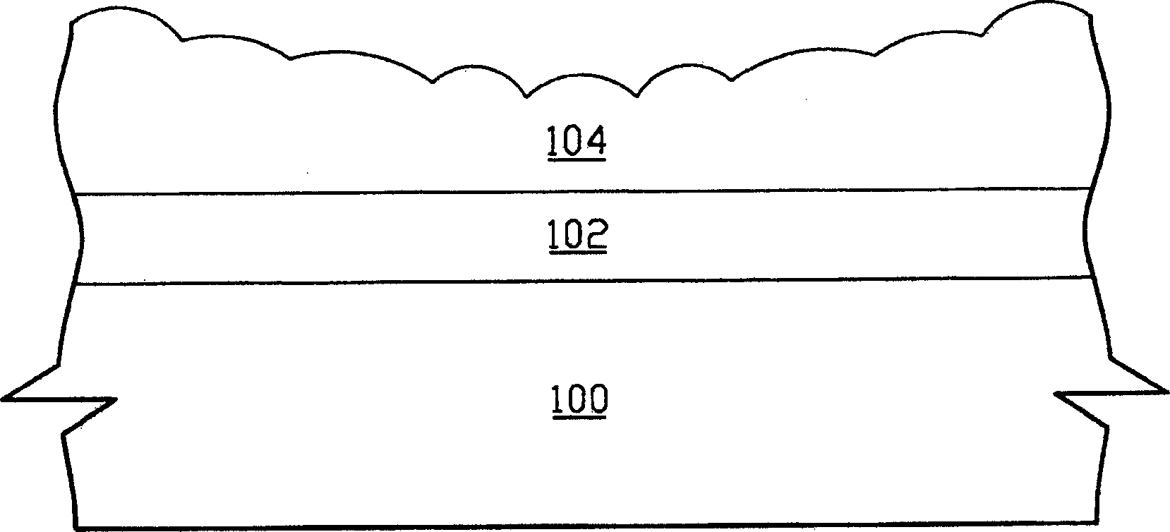
[0014] The polysilicon gate depletion effect is the effect of carrier depletion in gates formed of semiconductor materials such as doped polysilicon gates. The effect of carrier depletion in the polysilicon gate occurs because an external electric field causes a region in which the doped polysilicon gate is attracted or repelled by the electric field without ionized dopants, that is, there is no free hole or free A vacant region where electrons appear. In the N-type polysilicon gate, the depletion region contains the donor (Donor), which cannot provide free electrons, while in the P-type polysilicon gate, the depletion region contains the acceptor (Acceptor), which cannot provide free holes. The carrier depletion effect of the polysilicon gate will lead to a decrease in the electric field strength when the voltage is applied to the polysilicon gate. This phenomenon also means that the control ability of the gate is weakened, which will lead to the carrier concentration and dev...


PUM


Abstract

The invention reveals a method for forming polycrystalline silicon germanium layer, using chemical gas-phase chemical precipitation, which uses Si2H6 (Disilane) and germanium containing gas as a precursor to make the reaction between 500 deg.C and about 600 deg.C, to form a polycrystalline silicon germanium layer on a gate dielectric layer as a gate. And the said polycrystalline silicon germanium layer is directly formed on the gate dielectric layer and provided with a uniform and flat surface.

Description

technical field [0001] The invention relates to a method for forming a polysilicon germanium layer, especially a method for directly forming a polysilicon germanium layer on an oxide layer without pre-forming a polysilicon seed layer (polysilicon seed layer). Background technique [0002] The rapid development of semiconductor manufacturing technology has allowed millions or even more circuit elements such as transistors to be laid out on a single integrated circuit chip. In order to achieve such a high device integration, not only the line width of the integrated circuit must be greatly reduced, but also the size of the common Metal-Oxide-Semiconductor Field Oxide Transistor (MOSFET) must be reduced. Metal-oxide-semiconductor field-effect transistors are also known as isolated gate field-effect transistors (Insulated Gate FieldOxide Transistor, IGFET), but most of the time they are called field-effect transistors. [0003] The miniaturization of field effect transistors is...

Claims


Application Information

Patent Timeline
IPC IPC(8): H01L21/205H01L21/285
Inventor 褚国栋程立伟
Owner UNITED MICROELECTRONICS CORP
Features
  • R&D
  • Intellectual Property
  • Life Sciences
  • Materials
  • Tech Scout
  • Unparalleled Data Quality
  • Higher Quality Content
  • 60% Fewer Hallucinations
Learn More