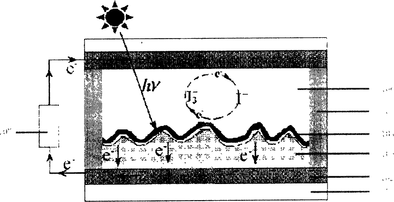
Large area internal series dye sensitization nano-thin film solar cell and producing method thereof
A technology for solar cells and dye sensitization, applied in the field of solar cells, can solve problems such as difficulty in material selection, achieve high output current, avoid stability problems and industrialization technical problems, and overcome technical difficulties and material selection difficulties.
- Summary
- Abstract
- Description
- Claims
- Application Information
AI Technical Summary
Problems solved by technology
Method used
Image
Examples
Embodiment 1
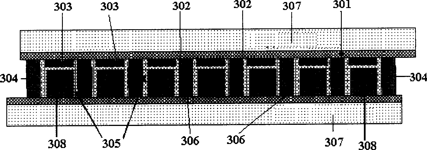
[0034] See attached picture.
[0035] 1. Conductive glass preparation: Select conductive glass as the transparent conductive electrode material (TEC-15, 3 mm, LOF, USA), cut into 10 cm × 10 cm, clean and set aside.
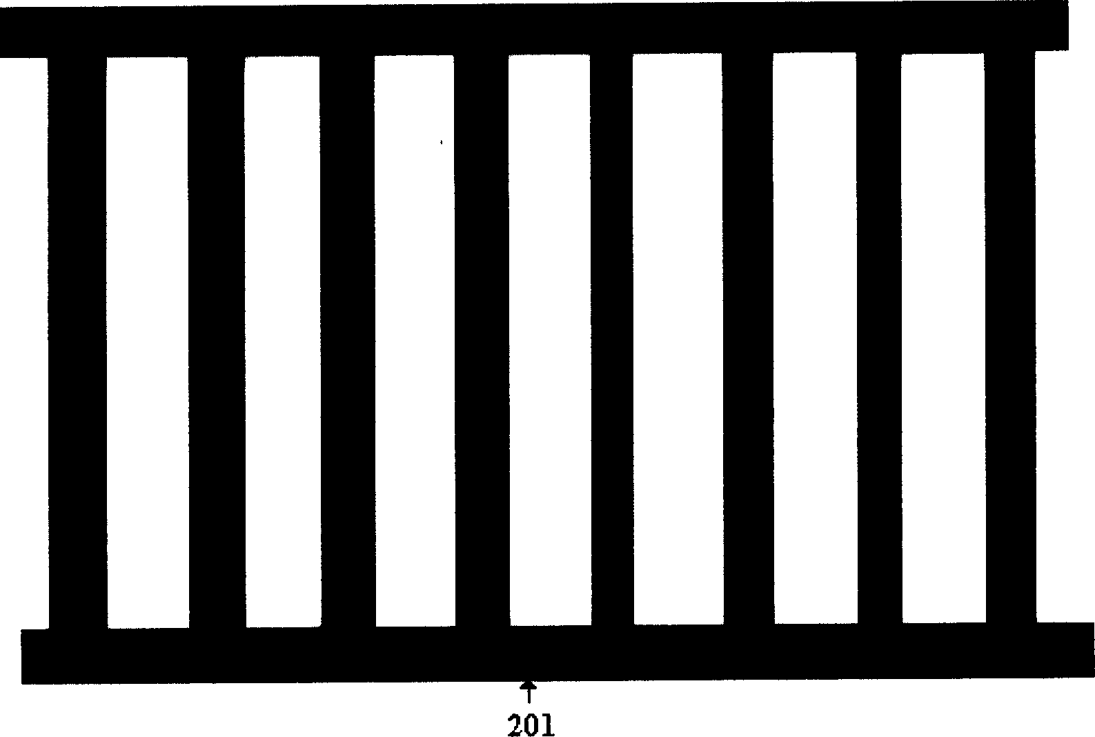
[0036] 2. Parallel electrode printing: Use screen printing technology to evenly print comb-shaped silver electrodes (such as: FERRO, CN33-246), sinter at 500 degrees Celsius (500 degrees Celsius for 30 minutes), the width of the silver electrode is about 1.5 mm, and the thickness is about 20 microns , a total of 8 items. Use screen printing silver brush glass paste on the silver electrode, so that the glass paste completely protects the silver electrode (where the wide-side silver electrode is exposed), and the total width of each protected electrode after sintering at 550 degrees Celsius (550 degrees Celsius for 30 minutes) About 3 mm and a thickness of about 30 microns.
[0037] 3. Photoanode (negative electrode) preparation: printing nano-TiO 2 Slurry, sinteri...
Embodiment 2
[0042] See attached picture.
[0043] 1. Conductive glass preparation: Select conductive glass as the transparent conductive electrode material (TEC-15, 3 mm, LOF, USA) and cut it into 10 cm × 10 cm, clean and set aside.
[0044] 2. Parallel electrode printing: Use screen printing technology to uniformly print comb-shaped silver electrodes (FERRO, CN33-246), sinter at 500 degrees Celsius (30 minutes at 500 degrees Celsius), the width of the silver electrode is about 1.5 mm, and the thickness of the silver electrode is about 20 microns , a total of 8 items.
[0045] 3. Photoanode (negative electrode) preparation: screen printing nano-TiO 2 Slurry, sintered at 500 degrees Celsius (500 degrees Celsius for 30 minutes) to become nanoporous TiO 2 Thin film, about 10 microns thick.
[0046] 4. Photocathode (positive electrode) preparation: According to the size and pattern required by the design, on another piece of conductive glass that has completed parallel electrodes, screen p...
Embodiment 3
[0050] See attached picture.
[0051] 1. Conductive glass preparation: Select conductive glass as the transparent conductive electrode material (TEC-15, 3 mm, LOF, USA) and cut it into 10 cm × 10 cm, clean and set aside.
[0052] 2. Parallel electrode printing: Use screen printing technology to uniformly print comb-shaped silver electrodes (FERRO, CN33-246), sinter at 500 degrees Celsius (30 minutes at 500 degrees Celsius), the width of the silver electrode is about 1.5 mm, and the thickness of the silver electrode is about 20 microns , a total of 8 items.
[0053] 3. Photoanode (negative electrode) preparation: printing nano-TiO 2 Slurry, sintered at 500 degrees Celsius (500 degrees Celsius for 30 minutes) to become nanoporous TiO 2 Thin film, about 10 microns thick. At a concentration of 0.5mM cis-(SCN - ) 2 Bis(2,2'-bipyridyl-4,4'-dicarboxylate) ruthenium(II) dye was soaked for a day and night, after taking it out, it was washed with ethanol (analytical grade), and dri...
PUM
| Property | Measurement | Unit |
|---|---|---|
| Thickness | aaaaa | aaaaa |
| Thickness | aaaaa | aaaaa |
| Width | aaaaa | aaaaa |
Abstract
Description
Claims
Application Information


