Ministructure gas sensor array chip and its preparing method

A technology of gas sensor and array chip, which is applied in the field of gas sensor, can solve the problems of high power consumption of metal oxide sensor and hinder the popularization and application of gas sensor, and achieve good high temperature resistance, improved stability, and simplified processing technology Effect

Inactive Publication Date: 2005-10-19
INST OF ELECTRONICS CHINESE ACAD OF SCI
View PDF0 Cites 26 Cited by
  • Summary
  • Abstract
  • Description
  • Claims
  • Application Information

AI Technical Summary

Problems solved by technology

Since most metal oxide gas sensing materials (SnO 2 , ZnO, Fe 2 o 3 etc.) need to work at a temperature of about 150-450, which makes the power consumption of the metal oxide sensor relatively large (generally 0.5W-1W), and the selectivity of this gas sensor can only be achieved by doping, catalysis and selection of the best Working temperature and other methods to optimize, can not fundamentally solve
These defects hinder the popularization and application of gas sensors; especially in aerospace, environmental monitoring and building safety, there is an urgent demand for low-power microstructure gas sensors and arrays

Method used


Image

  • Ministructure gas sensor array chip and its preparing method
  • Ministructure gas sensor array chip and its preparing method
  • Ministructure gas sensor array chip and its preparing method

Examples


Embodiment Construction

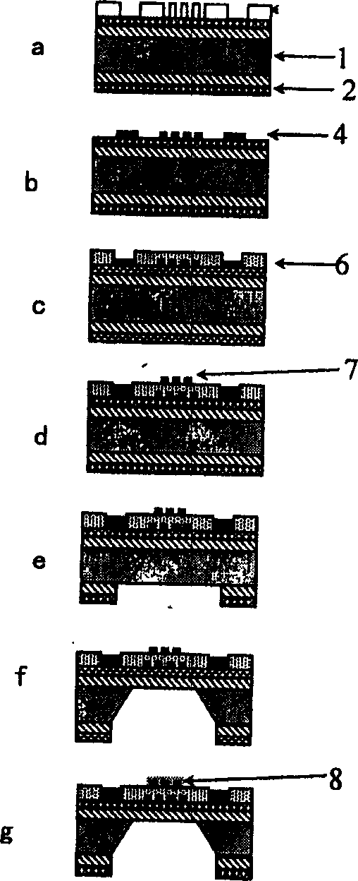
[0042] The concrete implementation method of the present invention is described in conjunction with accompanying drawing:

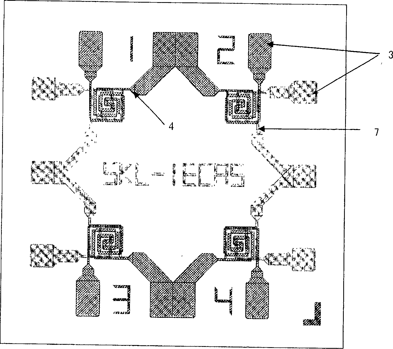
[0043] figure 1 It is a schematic diagram of the diaphragm structure of one of the units of the present invention. In the figure, 4 is a heating electrode, 7 is a measuring electrode, and 3 is a pressure welding block. Each unit of the present invention has independent heating electrode 4, is convenient to adjust the working temperature of each unit of the present invention; The current density of the electrodes is greater than that of the electrodes in the central area, and the corresponding heat generation is also relatively large, which improves the temperature uniformity of the working areas of each unit (the area with the gas-sensitive film).

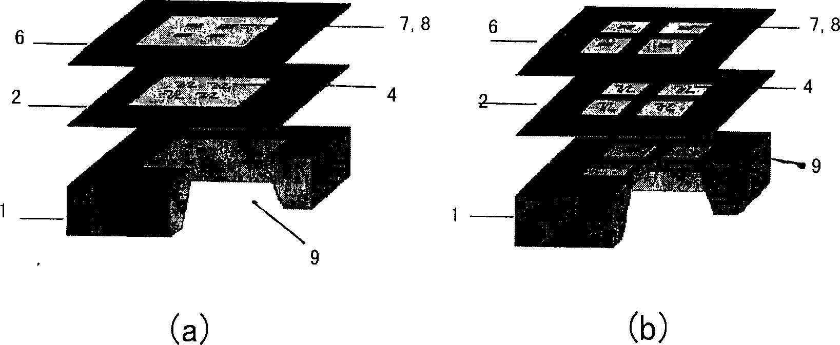
[0044] figure 2 It is a structural schematic diagram of two specific embodiments of the microstructure gas sensor array of the present invention. Among them, (a) is a single-diaphragm structure, and (b) i...


PUM

PropertyMeasurementUnit
thicknessaaaaaaaaaa
thicknessaaaaaaaaaa
thicknessaaaaaaaaaa

Abstract

This invention relates to a chip structure of a microstructure gas sensing sensor array and a preparation method. Said chip is composed of a silicon chip, a heating electrode, a measuring electrode and a gas sensitive film, among which, more than one independent through-holes are set at the center of the base silicon chip and are covered with a supporting film and an insulation film, a heating electrode is set in the supporting film center, the insulation film center has a measuring electrode covered with the gas sensitive film, the insulation film is set between the heating electrode and measuring electrode, the heating electrodes and the gas sensitive films are set opposite to the through-holes. This invention produces large quantities of microstructure gas sensitive sensor arrays with MEMS technology taking metal film as the heating electrode and measuring electrode to greatly increase its stability.

Description

technical field [0001] The invention belongs to the technical field of gas sensitive sensors, and in particular relates to a chip structure and a preparation method of a microstructure gas sensitive sensor array. Background technique [0002] Gas sensors have been widely used in environmental monitoring, disaster prevention alarm, chemical industry, food processing and other fields. Among various gas sensors, metal oxide sensors have attracted attention due to their simple structure and low price. Since most metal oxide gas sensing materials (SnO 2 , ZnO, Fe 2 o 3 etc.) need to work at a temperature of about 150-450, which makes the power consumption of the metal oxide sensor relatively large (generally 0.5W-1W), and the selectivity of this gas sensor can only be achieved by doping, catalysis and selection of the best The working temperature and other methods are optimized, which cannot be solved fundamentally. These defects hinder the popularization and application of ...

Claims


Application Information

Patent Timeline
Patent Type & Authority Applications(China)
IPC IPC(8): G01N27/12H01L49/00
Inventor 高晓光李建平何秀丽王利
Owner INST OF ELECTRONICS CHINESE ACAD OF SCI
Why Eureka
Try Eureka