Techniques for fabricating a resistor on a flexible base material

A technology for resistors and flexible substrates, applied in the direction of resistors, thin film resistors, and printed resistors

Inactive Publication Date: 2005-11-09
GENERAL ELECTRIC CO
View PDF0 Cites 7 Cited by
  • Summary
  • Abstract
  • Description
  • Claims
  • Application Information

AI Technical Summary

Problems solved by technology

However, for semiconductor devices fabricated on flexible substrate materials, fabricating resistors may present certain challenges
Typically, it is difficult to fabricate small, high resistance (range 100k ohm - 1M ohm) thin film resistors on flexible substrate materials such as polyimide

Method used


Image

  • Techniques for fabricating a resistor on a flexible base material
  • Techniques for fabricating a resistor on a flexible base material
  • Techniques for fabricating a resistor on a flexible base material

Examples


Embodiment Construction

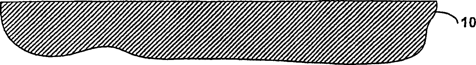
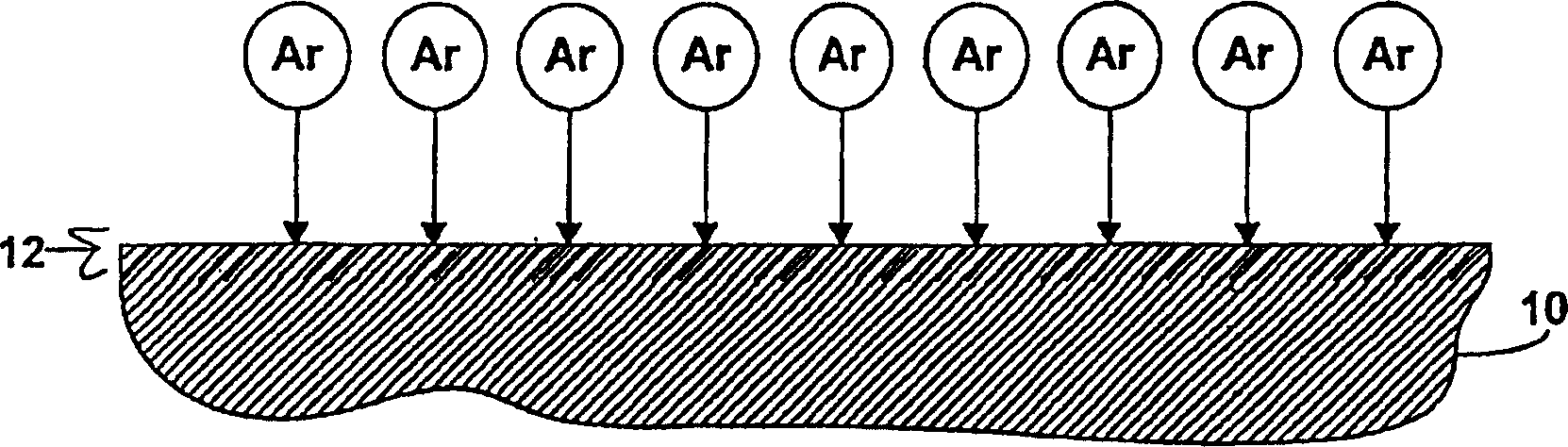
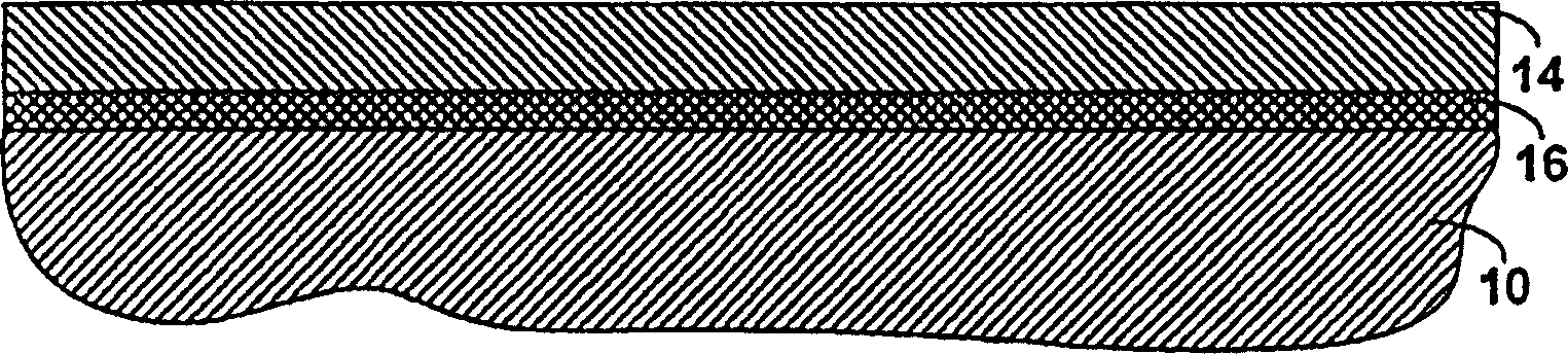
[0014] Now, will refer to Figure 1-6A , a first exemplary technique for fabricating high resistance resistors (in the range of 100k ohms - 1M ohms) on flexible substrate materials is described. figure 1 The flexible substrate material 10 on which the resistors are to be fabricated is illustrated. The flexible substrate 10 has a thickness of 0.5-3 mils and comprises a flexible plastic sheet that can be bent into a desired shape. A flexible substrate capable of bending or flexing is defined as a film or composition having a modulus of elasticity not exceeding 10,000 PSI at 23 degrees Celsius as tested by the standard flexural strength method. The flexible substrate material 10 is an electrically insulating material, preferably comprising a polymer film to which a conductive material can be adhered. The flexible substrate material 10 includes a modulus of elasticity, a coefficient of thermal expansion, and a coefficient of moisture expansion that minimize dimensional changes d...


PUM

PropertyMeasurementUnit
elastic modulusaaaaaaaaaa
thicknessaaaaaaaaaa
thicknessaaaaaaaaaa

Abstract

A technique for fabricating a resistor on a flexible substrate (10) (28). Specifically, at least a portion of a polyimide substrate (10) (28) is activated by exposure to a ion sputter etch techniques. A metal layer (14) (36) is depositing over the activated portion (12) (34) of the substrate (10) (28), thereby resulting in the formation of a highly resistive metal-carbide region (16) (38). Interconnect layers (18, 20) (40, 42) are deposited over the metal-carbide region (16) (38) and patterned to form terminals (24, 26) (44, 46) at opposite ends of the metal carbide region (l6) (38). The metal-carbide region (16) (38) is patterned to form a resistor between the terminals. Alternatively, only a selected area of the polyimide substrate (10) (28) is activated. The selected area forms the area in which the metal-carbide region (16) (38) is formed. Interconnect layers (18, 20) (40, 42) are disposed over the metal-carbide region (16) (38) and patterned to form terminals (24, 26) (44, 46) at opposite ends of the metal-carbide region (16) (38).

Description

technical field [0001] The present invention relates generally to the fabrication of resistors, and more particularly to high resistance structures formed on flexible substrate materials and techniques for fabricating such structures. Background technique [0002] Many commercial applications employ semiconductor devices that are susceptible to electrostatic discharge. A semiconductor light-emitting diode (LED) is one such device. LEDs are semiconductor chips that are packaged to emit radiation in response to an applied voltage or current. These LEDs are used in many commercial applications such as automotive, display, security / crisis, and directional area lighting. LEDs can be fabricated from any material that emits visible, ultraviolet or infrared radiation. Accordingly, the LED device may comprise a material having a p-n junction of the semiconductor layers and capable of emitting the desired radiation. For example, LED devices can be fabricated using any desired semi...

Claims


Application Information

Patent Timeline
Patent Type & Authority Applications(China)
IPC IPC(8): B29C59/14H01C7/00H01C17/12H05K1/03H05K1/16H05K3/38
CPCH05K2201/0317H05K1/167H05K2203/095H05K1/0346H05K3/381B29C59/14H01C17/12H05K2203/1136H05K3/388H05K2201/0154H01C7/006H01C3/06
Inventor 凯文·M·杜罗彻理查德·J·塞亚维克拉姆·B·克里什纳默西
Owner GENERAL ELECTRIC CO
Why Eureka
Try Eureka