Resistive cell structure for reducing soft error rate and inverter and forming method

A storage unit and soft error technology, applied in static memory, digital memory information, electrical components, etc., can solve problems such as data integrity loss, and achieve the effect of prolonging the delay time

Inactive Publication Date: 2005-11-16
TAIWAN SEMICON MFG CO LTD
View PDF0 Cites 4 Cited by
  • Summary
  • Abstract
  • Description
  • Claims
  • Application Information

AI Technical Summary

Problems solved by technology

[0004] However, when the semiconductor memory requires smaller area and higher mobility, the space saving of semiconductor memory becomes more and more important, especially in order to continue to obtain the benefits of size and performance, the memory cell must continue to shrink, however, the memory cell When shrinking, there is a problem. In the static random access memory unit, each inverter storage node is composed of the gate capacitance of the two transistors of the inverter. When the memory cell shrinks, the storage capacitor also shrinks. , the charge used to store data is so small that the electronic noise on the bit or word line or the charge induced by alpha particles (α-particles) becomes very significant in comparison. This electronic noise (which may be The frequency of errors caused by alpha particles) is the soft error rate. When the soft error rate increases, the risk of data integrity loss also increases. Therefore, noise tolerance has become an increasingly important issue in semiconductor memory design. areas of emphasis

Method used


Image

  • Resistive cell structure for reducing soft error rate and inverter and forming method
  • Resistive cell structure for reducing soft error rate and inverter and forming method
  • Resistive cell structure for reducing soft error rate and inverter and forming method

Examples


Embodiment Construction

[0037] In order to make the above-mentioned and other objects, features and advantages of the present invention more comprehensible, the preferred embodiments are listed below, together with the accompanying drawings, and are described in detail as follows:

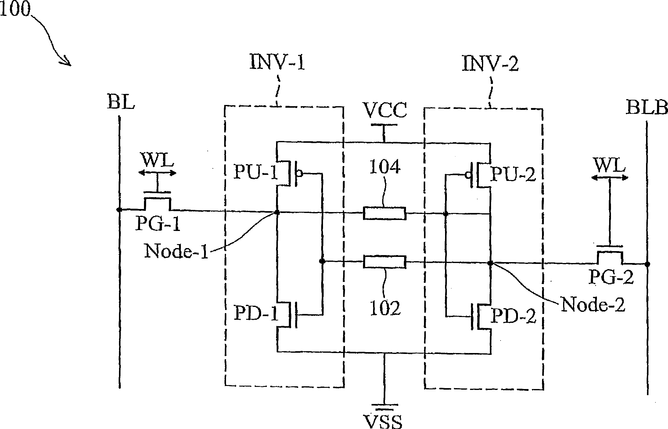
[0038] The present invention provides a design of a static random access memory unit with two resistors to reduce the soft error rate, thereby improving noise tolerance and data integrity. In several embodiments shown below, a standard static random access memory cell is modified by adding two resistors. Adding resistors increases the resistance / capacitance delay time (RC delay) required to change the stored data. Due to the standard static The two inverters of the random access memory unit are interactively coupled, and the impact of the return will also be delayed. The delay time can make the affected inverter self-compensate and maintain the original data, so it can reduce the noise caused by alpha particles The freque...


PUM


Abstract

A memory cell for reducing soft error rate and the method for forming same are disclosed. The memory cell comprises a first bit line signal (BL), a second bit line signal complementary to the first bit line signal (BLB), a first pass gate coupled to the BL, a second pass gate coupled to the BLB, a first inverter whose output node receives the BL through the first pass gate, a second inverter whose output node receives the BLB through the second pass gate, a first instrument coupled between the output node of the first inverter and an input node of the second inverter and a second instrument coupled between the output node of the second inverter and an input node of the first inverter, wherein the first and second instruments increase voltage discharge time of the memory cell when voltages at the output nodes of the inverters accidentally discharge.

Description

technical field [0001] The present invention relates to a semiconductor memory, and more particularly to improving the soft error rate with a high-resistance memory cell structure. Background technique [0002] A semiconductor memory is composed of an array of memory cells, and each memory cell stores a bit 1 or 0 in a high or low voltage state. At least every eight bits may constitute a byte, and at least every sixteen bits may constitute a character. In each memory operation cycle, usually at least one byte will be written into or read out of the memory array, and the memory cell is located at the junction of the vertical data line (or bit line) and the horizontal word line, which can be used to read Or write is enabled, and the read or write cycle occurs when a word line and a pair of bit lines are activated, and the memory cell located at the junction of the bit line and the word line can receive written data from the bit line or The read data is sent to the bit lines,...

Claims


Application Information

Patent Timeline
Patent Type & Authority Applications(China)
IPC IPC(8): G11C7/00G11C7/02G11C11/412H01L21/8244H01L27/10H01L27/11
CPCH01L27/1104G11C7/02H01L27/1112G11C11/4125H01L27/11H10B10/15H10B10/00H10B10/12
Inventor 廖忠志
Owner TAIWAN SEMICON MFG CO LTD
Why Eureka
Try Eureka