

Organic field effect transistor with an organic dielectric
A technology of organic fields and organic semiconductor layers, applied in the field of disordered or semi-disordered organic semiconductors, insulating materials of organic FETs, and organic semiconductors
Inactive Publication Date: 2010-11-10
MERCK PATENT GMBH
View PDF18 Cites 0 Cited by
- Summary
- Abstract
- Description
- Claims
- Application Information
AI Technical Summary
Problems solved by technology
The existing technology solves interface traps by using high dielectric constant insulators to induce high charge density to fill interface traps
Method used
View moreImage
Smart ImageViewing Examples


Examples
preparation example Construction
Embodiment 1
Embodiment 2
Login to View More PUM
 Abstract
A process of manufacturing an organic field effect device is provided comprising the steps of (a) depositing from a solution an organic semiconductor layer; and (b) depositing from a solution a layer of low permittivity insulating material forming at least a part of a gate insulator, such that the low permittivity insulating material is in contact with the organic semiconductor layer, wherein thelow permittivity insulating material is of relative permittivity from 1.1 to below 3.0. In addition, an organic field effect device manufactured by the process is provided.
Description
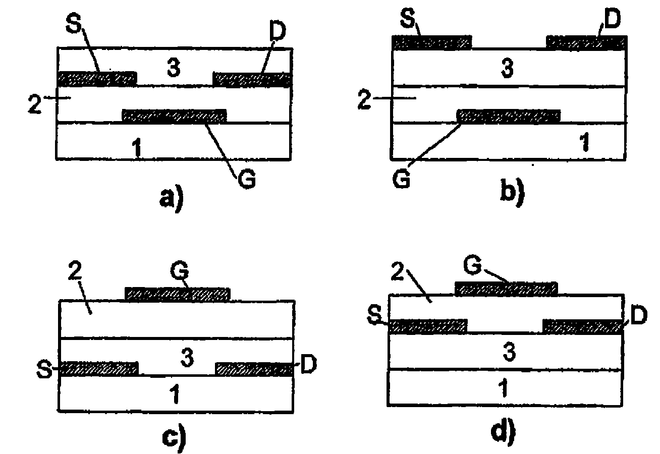
Organic Field Effect Transistors Using Organic Dielectrics Background of the invention The present invention relates to organic field effect transistors (OFETs) and methods for their manufacture. In the microelectronics industry, field effect transistors (FETs) based on inorganic materials such as Si are well established. A typical FET consists of many layers, which can be constructed in a variety of different ways. For example, a FET may include a body, an insulator, a semiconductor, source and drain electrodes connected to the semiconductor, and a gate electrode adjacent to the insulator. When a potential is applied to the gate electrode, carriers are gathered at the interface between the semiconductor and the insulator in the semiconductor, and as a result, a conductive channel is formed between the source electrode and the drain electrode. potential, a current flows. Over the past decade, the use of organic materials to study FETs has continued to gain momentum. The...
Claims
Login to View More Application Information
Patent Timeline
 Patent Type & AuthorityPatents(China)
IPC IPC(8): H01L51/20
InventorS・W・李明S・莫希亚尔丁-哈法夫S・D・奥吉尔J・弗雷斯
OwnerMERCK PATENT GMBH