
A coaxial interference surface plasmon microscopy method and system without pupil modulation

A technology of interfering surfaces and plasmas, applied in the direction of material analysis, instruments, and measuring devices through optical means, to achieve the effect of weakening requirements, simple system structure, and improved signal-to-noise ratio

Inactive Publication Date: 2019-09-17
BEIHANG UNIV
View PDF4 Cites 0 Cited by
  • Summary
  • Abstract
  • Description
  • Claims
  • Application Information

AI Technical Summary

Problems solved by technology

The disadvantage of this technology is that its lateral resolution is limited by the propagation length of the SPR wave, usually more than ten microns, which is much larger than the diffraction limit of conventional optical systems, that is, on the order of half a wavelength. A typical system is a prism-type SPR microscope system

Method used


Image

  • A coaxial interference surface plasmon microscopy method and system without pupil modulation
  • A coaxial interference surface plasmon microscopy method and system without pupil modulation
  • A coaxial interference surface plasmon microscopy method and system without pupil modulation

Examples


specific Embodiment approach 1

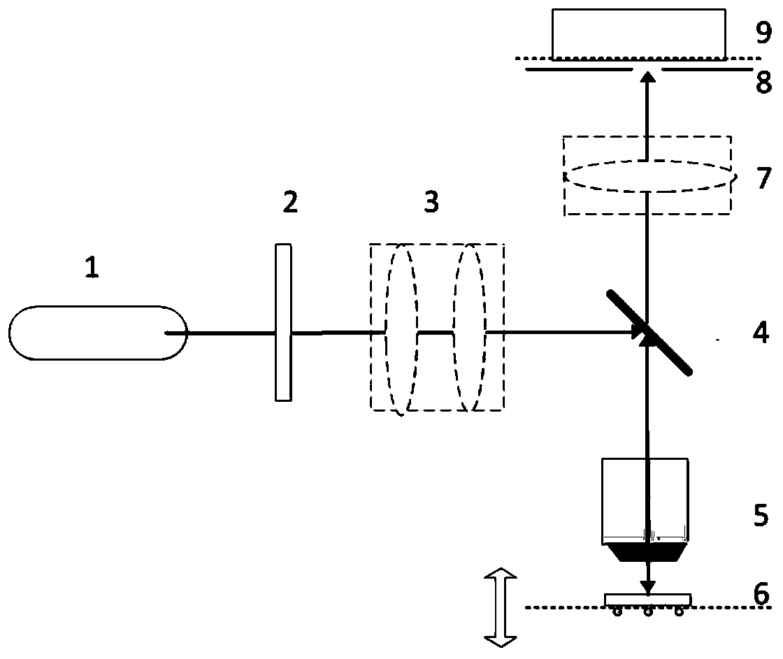
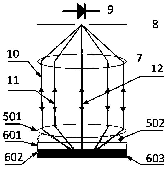
[0036] Specific implementation mode one: combine Figure 1 to Figure 4 Describe this embodiment mode, a coaxial interference surface plasmon microscope system without incident light modulation described in this embodiment mode, it includes: a laser transmitter (1), a polarization modulation device (2), a beam expander device (3 ), dichroic prism (4), microscope objective lens (5), cover glass with sample (6), imaging lens (7), confocal diaphragm (8), image sensor (9).

[0037] The centers of the laser transmitter (1), polarization modulation device (2), beam expander (3) and beam splitting prism (4) are located on the same optical axis; microscope objective lens (5), cover glass with sample (6) , the imaging lens (7), the confocal diaphragm (8) and the image sensor (9) are located on the same optical axis.

[0038] The polarization modulation device (2) generally consists of a half glass and a polarizer, and the photosensitive surface of the image sensor (9) is conjugate to t...

specific Embodiment approach 2

[0053] Embodiment 2: The system layout of this embodiment is as described in Embodiment 1, but this embodiment provides a method for quickly scanning the surface microtopography of a sample.

[0054] Such as Figure 7 As shown in , select the point with the largest difference between the two V(z) curves, control the micro-nano mobile scanning device to fix the defocus distance, and then perform two-dimensional scanning on the sample to be tested to obtain the surface micromorphology of the sample appearance. In this implementation manner, the imaging contrast can be controlled by selecting different defocus distances.


PUM


Abstract

The invention discloses a pupil modulation-free coaxial interference surface plasma microscopy method and system. The system comprises a coherent illumination light source, a polarization modulation device, a beam expanding device, a sample clamping device, a micro-nano mobile scanning device, a confocal aperture, an imaging lens group and an image sensor and the above parts are orderly arranged along a light path. In the sample defocusing process, the image sensor conjugated to the focal plane of a microscope objective detects an interference signal which forms a V(z) curve. The clear aperture of the system is limited so that the edge disturbance effect is caused and influences the period of the V(z) curve. The influence is eliminated through notch filtering. The bandwidth and center frequency of a notch filtering device are linearly related to the numerical aperture of the system. The system realizes half-wavelength and sub-nanometer ultra-microscopic detection of lateral and axial resolution ratios and has the advantages of no pupil modulation, simple system, low cost and fast high-resolution imaging.

Description

technical field [0001] The invention relates to the field of nanometer optical detection, in particular to a coaxial interference surface plasma microscope system free from incident light modulation. [0002] Background of the invention [0003] Surface plasmon (SPR) is an electromagnetic wave that propagates along the surface of metals and dielectrics. It is very sensitive to changes in the refractive index and thickness of metals and electrolytes. New nanomaterials, molecular-molecular interactions, etc. are detected, and the detection results have outstanding accuracy, stability and high repeatability, and are widely used in chemistry, medical treatment, biology, semiconductor materials, information and other fields. The disadvantage of this technology is that its lateral resolution is limited by the propagation length of the SPR wave, usually more than ten microns, which is much larger than the diffraction limit of conventional optical systems, that is, on the order of ha...

Claims


Application Information

Patent Timeline
Patent Type & Authority Patents(China)
IPC IPC(8): G01N21/552
Inventor 张蓓刘雨张承乾荆嘉玮闫鹏
Owner BEIHANG UNIV
Learn More