Method for producing a stepped edge profile comprised of a layered construction
A step-and-configuration technology, applied in semiconductor/solid-state device manufacturing, electrical components, electric solid-state devices, etc., can solve the problems of adverse effects on semiconductor chip performance, damage, and difficulty in removal, so as to achieve environmentally friendly implementation, Economical implementation, reduced complexity effects
- Summary
- Abstract
- Description
- Claims
- Application Information
AI Technical Summary
Problems solved by technology
Method used
Image


Examples
Embodiment Construction
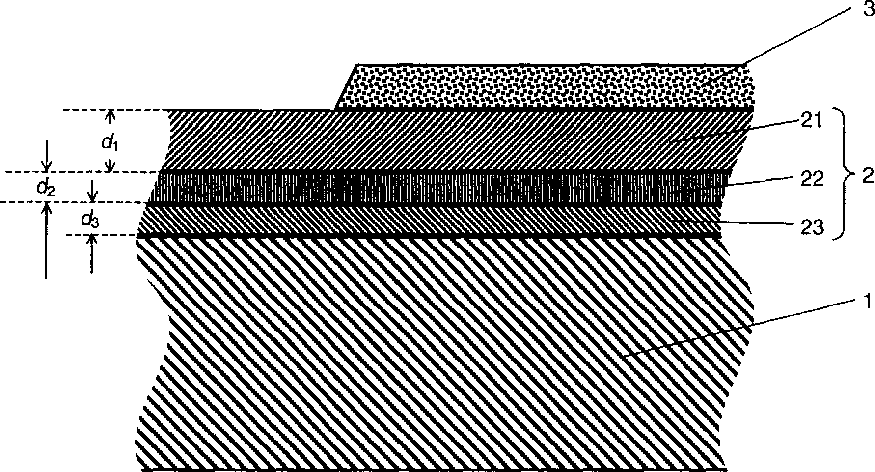
[0017] The symbols used in the drawings and their meanings are summarized in the symbol table. In principle, the same reference numerals denote the same parts.
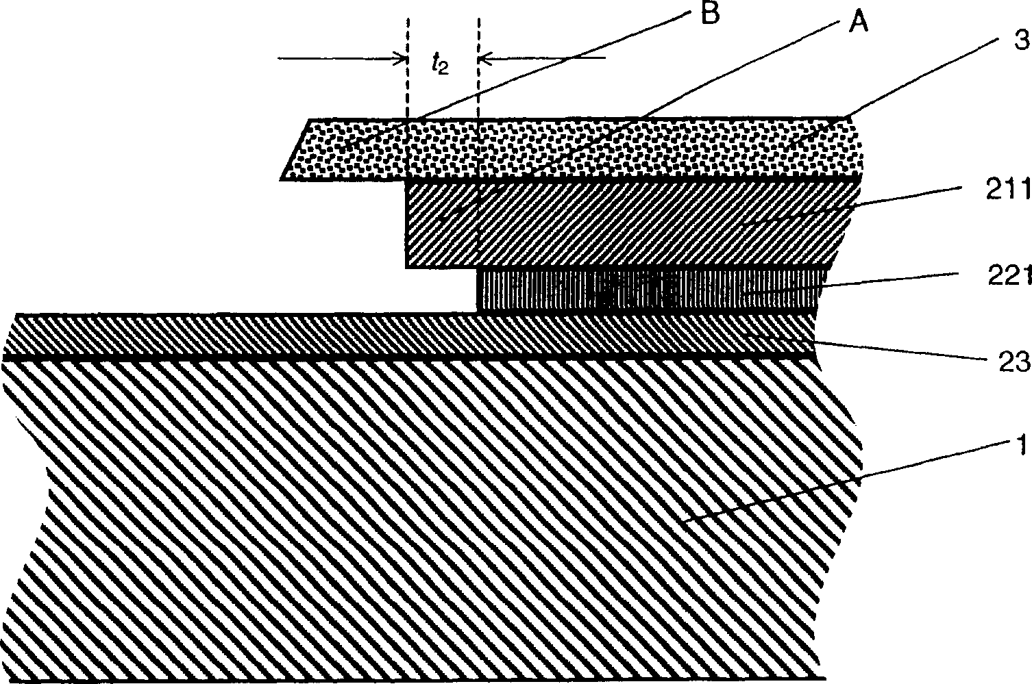
[0018] figure 1 The initial product of the method according to the invention is shown, comprising a layer array 2 laid on a semiconductor chip 1, said layer array 2 consisting of an Ag layer (aluminum layer) 21 as a first layer, an Ag layer (aluminum layer) 21 as a second layer, A Ni layer (nickel layer) 22, and a Ti layer (titanium layer) 23 as a third layer are constituted. The first thickness d1 of the Ag layer 21 is preferably a few microns, the second thickness d2 of the Ni layer 22 and the third thickness d3 of the Ti layer are preferably a few tenths of a micron. Part of the Ag layer 21 is covered by a photosensitive varnish layer 3 as its protective layer.
[0019] In order to form a stepped configuration in Smeme 2, hydrogen peroxide (H 2 o 2 ), ammonium hydroxide (NH 4 OH) and water (H 2 The first che...
PUM
 Abstract
Description
Claims
Application Information
 - R&D
- Intellectual Property
- Life Sciences
- Materials
- Tech Scout
- Unparalleled Data Quality
- Higher Quality Content
- 60% Fewer Hallucinations
Browse by: Latest US Patents, China's latest patents, Technical Efficacy Thesaurus, Application Domain, Technology Topic, Popular Technical Reports.
© 2025 PatSnap. All rights reserved.Legal|Privacy policy|Modern Slavery Act Transparency Statement|Sitemap|About US| Contact US: help@patsnap.com