Method for eliminating stress and damage in producing monolithic photoelectric integrated receiver

A technology of optical receiver and photoelectric integration, applied in the field of optoelectronics, to achieve the effect of easy operation, not easy to stain, and improved annealing efficiency

Inactive Publication Date: 2006-01-04
UNIV OF ELECTRONIC SCI & TECH OF CHINA
View PDF0 Cites 3 Cited by
  • Summary
  • Abstract
  • Description
  • Claims
  • Application Information

AI Technical Summary

Problems solved by technology

[0011] In order to solve the above-mentioned problem of thermal annealing, we propose a method for eliminating stress and damage in the manufacture of monolithic optoelectronic integrated optical receivers. According to the method of the pr

Method used


Image

  • Method for eliminating stress and damage in producing monolithic photoelectric integrated receiver
  • Method for eliminating stress and damage in producing monolithic photoelectric integrated receiver
  • Method for eliminating stress and damage in producing monolithic photoelectric integrated receiver

Examples


Embodiment Construction

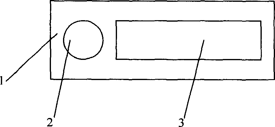
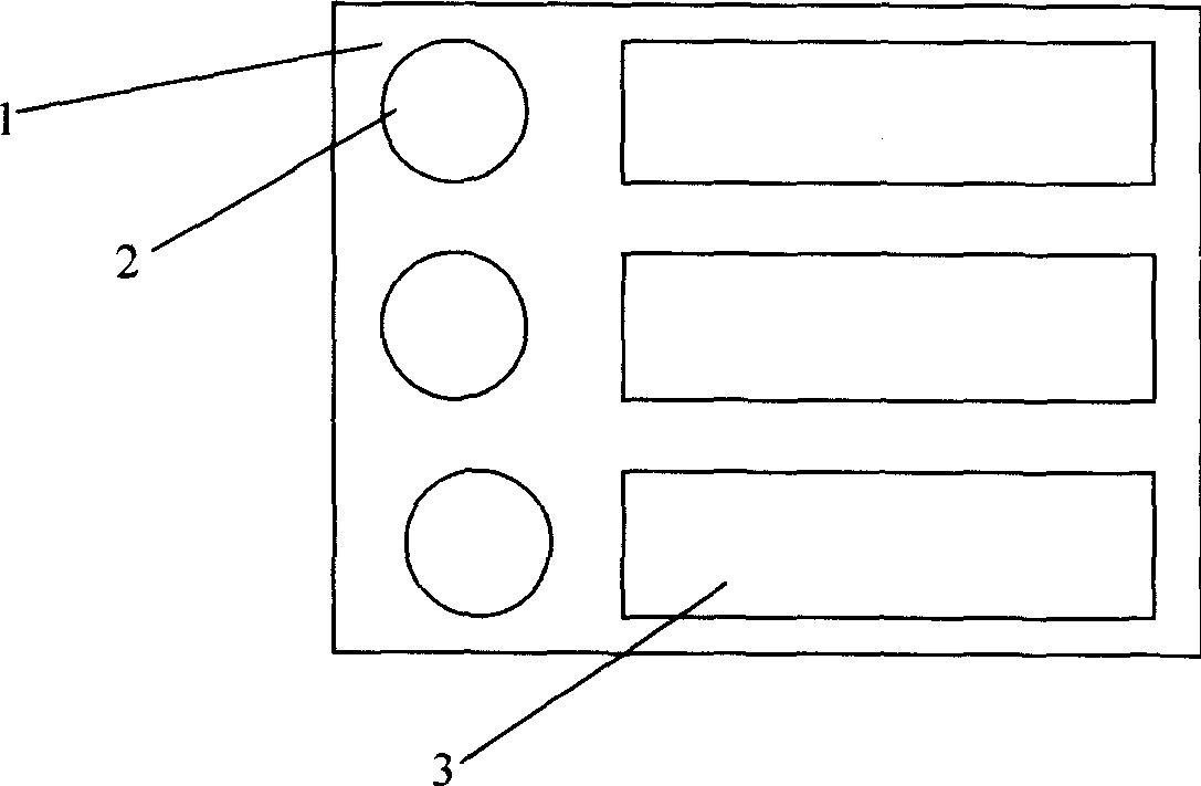
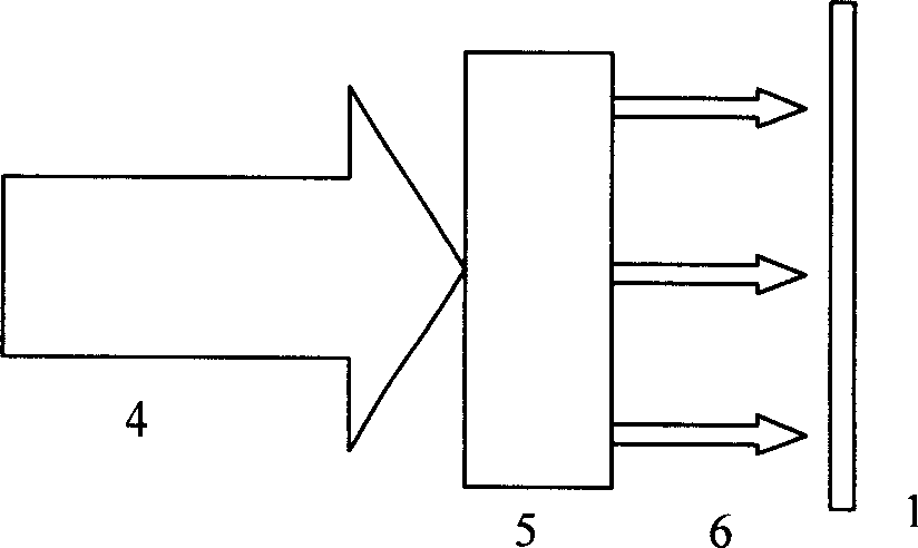
[0035] According to the annealing method provided by the present invention, a laser local annealing device (as attached Figure 4 shown), it is made up of a laser 7, a reflector 8, a lens 9, a substrate 10, a three-dimensional adjustment platform 11, a temperature measuring device 12, and a window 13 for transmitting laser light; the substrate 10 that has undergone ion implantation process is placed in On the three-dimensional adjustment table 11, the laser light emitted by the laser 7 is reflected by the mirror 8, and then focused by the lens 9 and irradiated on the substrate 10 for annealing to eliminate stress and damage after ion implantation. Adjusting the three-dimensional adjusting stage 11 through the window 13 for transmitting laser light can make the laser beam align with a certain photodiode area on the substrate. The annealing temperature can be measured by the temperature measuring device 12, and can be adjusted by adjusting the power of the incident laser beam. ...


PUM


Abstract

The present invention provides method of eliminating stress and damage of light receiver during monolithic photoelectronic integration. The area of semiconductor surface to be annealed is irradiated with laser beam of very high power density to produce abrupt temperature change process with great temperature change rate, short duration and proper range, so as to improve the performance of the semiconductor and eliminate defects, damage, etc. The method of the present invention is especially suitable for eliminating stress and damage of PDIC after ion implantation during monolithic PDIC manufacture.

Description

technical field [0001] The invention belongs to the field of optoelectronic technology, and in particular relates to laser application technology. Background technique [0002] In recent years, monolithic OEICs (Optoelectronics Integrated Circuits, referred to as OEICs) devices have developed rapidly, among which monolithic integrated PDIC (Photodiode / preamplifier Integrated Circuits, that is, photodiode / preamplifier integrated circuits) optical receivers (hereinafter Monolithic Integrated Optical Receiver or PDIC for short) is an important monolithic OEICs device, which manufactures photodiodes and preamplifier circuits on the same chip, and its front end is a photodiode that converts optical signals into electrical signals ; The back end is a pre-amplification circuit, which can amplify the photoelectric signal to the required amplitude. At present, monolithic integrated PDIC is mainly used in fields such as optical communication, laser precision guidance, optically contr...

Claims


Application Information

Patent Timeline
IPC IPC(8): H01L21/268H01L21/20B23K26/00
Inventor 叶玉堂吴云峰焦世龙张雪琴赵爱英刘霖王昱琳
Owner UNIV OF ELECTRONIC SCI & TECH OF CHINA
Why Eureka
Try Eureka