Photoresistive desquamation process and apparatus thereof

A stripping device and photoresist technology, applied in the field of semiconductor manufacturing process and device, can solve the problems of high operating cost, high production cost, low yield, etc., and achieve the effects of short rinsing process time, increase yield, and reduce aluminum erosion

Inactive Publication Date: 2006-01-18
HONG FU JIN PRECISION IND (SHENZHEN) CO LTD +1
View PDF1 Cites 6 Cited by
  • Summary
  • Abstract
  • Description
  • Claims
  • Application Information

AI Technical Summary

Problems solved by technology

[0015] In order to solve the problems of serious aluminum erosion, low yield and high production cost in the photoresist stripping process of the prior art, the present invention provides a photoresist stripping film that can effectively prevent aluminum erosion, has high yield and low production cost. Process
[0016] In order to solve the problems of aluminum erosion, low yield and high operating cost of the photoresist stripping device in the prior art, the present invention provides a photoresist stripping device that can effectively prevent aluminum erosion, have high yield and low operating cost device

Method used


Image

  • Photoresistive desquamation process and apparatus thereof
  • Photoresistive desquamation process and apparatus thereof
  • Photoresistive desquamation process and apparatus thereof

Examples


Embodiment Construction

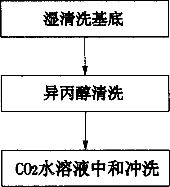
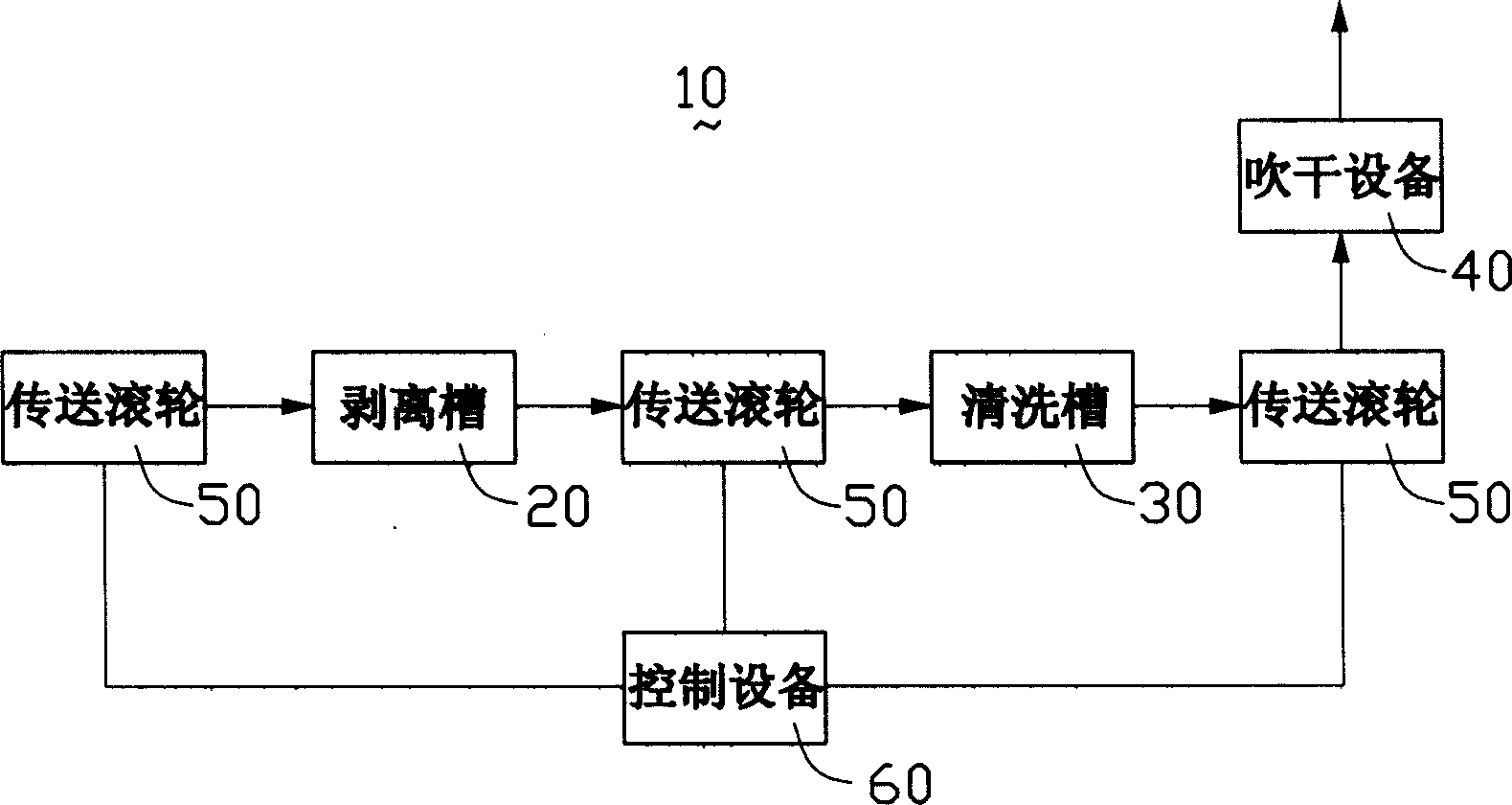
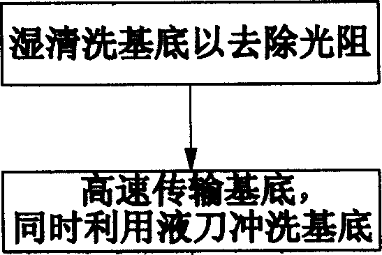
[0024] Such as figure 2 As shown, the photoresist stripping process of the present invention mainly includes two steps: (1) wet-cleaning the substrate; (2) transferring the substrate at high speed while rinsing the substrate with a liquid knife.

[0025] First, the substrate including the photoresist layer to be subjected to the photoresist stripping process is placed in a wet bench, and the photoresist stripping solution is sprayed onto the surface of the substrate. The photoresist stripping solution is an organic solvent, such as N-methylrolidone. The method of spraying the photoresist stripper can be spray coating or spin coating. The spraying method uses a nozzle to evenly spray the photoresist stripping solution onto the surface of the substrate, while the spin coating method puts the photoresist stripping solution on the substrate surface, and then rotates the substrate so that the photoresist stripping solution is evenly distributed on the substrate.

[0026] The pho...


PUM


Abstract

The invention provides an optical resistance stripping process which comprises the following steps: wet cleaning base to strip optical resistance, transmitting it with high speed and using Aqua Knife to clean base at the same time. The invention also provides an optical resistance-stripping device, which can be applied in optical resistance stripping steps of semiconductor process.

Description

【Technical field】 [0001] The invention relates to a semiconductor process and device, in particular to a photoresist stripping process and device. 【Background technique】 [0002] With the development of science and technology, the application of semiconductor manufacturing process is becoming more and more extensive. For example, the manufacturing process of liquid crystal display, organic light emitting diode and other products includes semiconductor manufacturing process. [0003] A typical semiconductor manufacturing process mainly includes photoresist coating (Photo-resist Coating), lithography (Lithography), development (Developing) and etching (Etching). Photoresist coating is to coat a photoresist layer on a substrate, including physical and chemical coating methods. Lithography is to use a mask with a specific pattern to transfer the pattern to the photoresist layer, and then develop it to expose the layer to be processed according to the specific pattern. Then the...

Claims


Application Information

Patent Timeline
Patent Type & Authority Applications(China)
IPC IPC(8): G03F7/42G03F7/26
Inventor 黄志鸿
Owner HONG FU JIN PRECISION IND (SHENZHEN) CO LTD
Why Eureka
Try Eureka