

Peeling method and method for manufacturing display device using the peeling method
A technology for a display device and a manufacturing method, applied to identification devices, lighting devices, instruments, etc., to achieve the effects of unbreakable, simplified manufacturing process, and light weight
- Summary
- Abstract
- Description
- Claims
- Application Information
AI Technical Summary
Problems solved by technology
Method used
Image

Examples
Embodiment approach 1
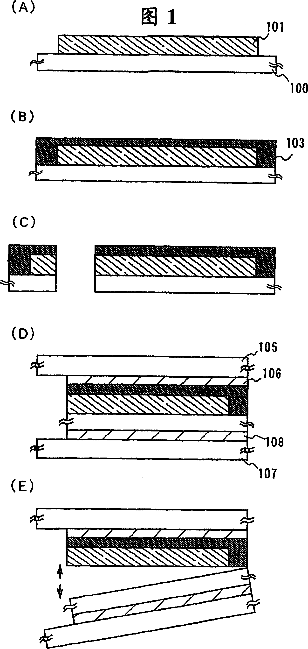
[0049] This embodiment describes an example of a specific peeling process when peeling and transferring the state after formation of the light-emitting element and liquid crystal element as the layer to be peeled, and manufacturing a light-emitting device that emits light from the top surface using the peeling process of the present invention.
[0050] like image 3 As shown in (A), the metal film 201 is formed on the first substrate 200 . In this embodiment, a glass substrate of about 0.5 to 1.0 mm is used as the first substrate. As the metal film, an alloy material or compound composed of elements selected from W, Ti, Ta, Mo, Nd, Ni, Co, Zr, Zn, Ru, Rh, Pd, Os, Ir or mainly composed of the above elements can be used. Single layers of materials or their laminates. As a method for producing the metal film, a sputtering method can be used to form the metal film on the first substrate using a metal as a target. In addition, the film thickness of the metal film is set to be 10...
Embodiment approach 2
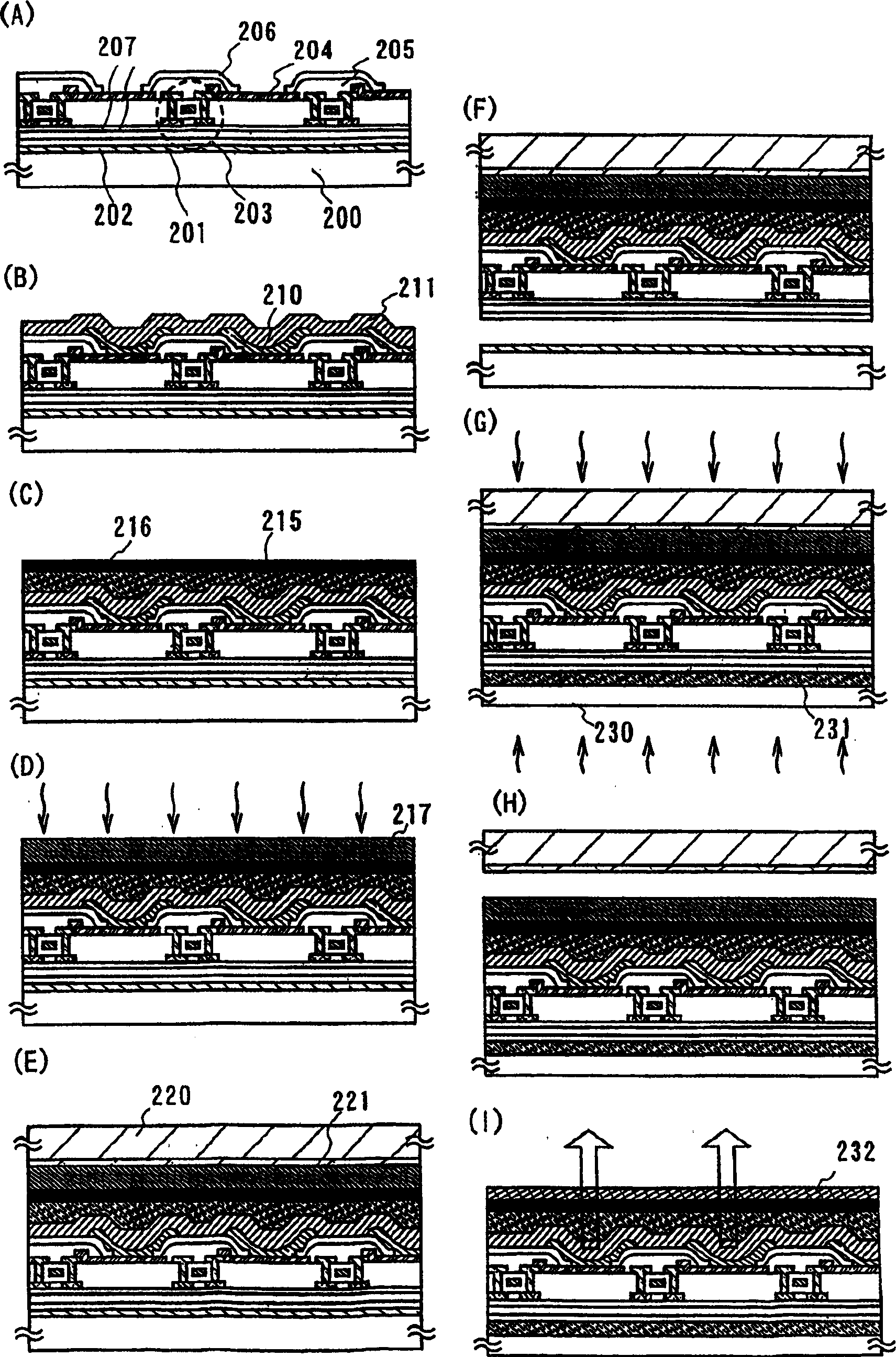
[0083] In this embodiment, the lower surface is formed by using the peeling process when the adhesive is controlled by applying ultraviolet rays and heat to the state after the formation of the light-emitting element and the liquid crystal element as the layer to be peeled, and performing peeling and transfer. An example of a light-emitting device that emits light will be described, and descriptions of steps and materials that are the same as those in Embodiment 1 will be omitted.
[0084] First, it is the same as Embodiment 1, until the protective film 215 is formed ( Figure 4 (A)). However, since it is a light-emitting device that emits light from the bottom surface, it is necessary to use a light-transmitting material for the electrode 204 . In addition, a stress relief member may be provided, but it is not particularly provided in this embodiment.
[0085] like Figure 4 As shown in (B), next, the second substrate 220 is fixed on the protective film 215 using the doubl...
Embodiment approach 3
[0092] In this embodiment mode, a description will be given of a method of manufacturing a light-emitting device in which a semiconductor element, an electrode, an insulating film, and the like are formed as a layer to be peeled, and then peeled and transferred.
[0093] like Figure 12 As shown in (A), the metal film 201 is formed on the first substrate 200 . In this embodiment, a glass substrate of about 0.5 to 1.0 mm is used as the first substrate. As the metal film, an alloy material or compound material composed of elements selected from W, Ti, Ta, Mo, Nd, Ni, Co, Zr, Zn, Ru, Rh, Pd, Os, Ir or mainly composed of the above elements can be used. composed of single layers or their stacks. A sputtering method is used as a method for producing the metal film, and a metal can be used as a target to be formed on the first substrate. In addition, the film thickness of the metal film is set to be 10 nm to 200 nm, preferably 50 nm to 75 nm.
[0094] If an alloy of the above met...
PUM
| Property | Measurement | Unit |
|---|---|---|
| thickness | aaaaa | aaaaa |
| thickness | aaaaa | aaaaa |
| thickness | aaaaa | aaaaa |
Abstract
Description
Claims
Application Information