LED structure with gallium nitride system
A technology based on light-emitting diodes and gallium nitride, applied in electrical components, circuits, semiconductor devices, etc., can solve the problems of large gaps in lattice constants, affecting the luminous efficiency of light-emitting diodes, and large mechanical stress
- Summary
- Abstract
- Description
- Claims
- Application Information
AI Technical Summary
Problems solved by technology
Method used
Image


Examples
no. 1 example
[0030] The first embodiment of the gallium nitride-based light-emitting diode structure of the present invention includes: a substrate 11, a buffer layer (buffer layer) 12, an n-type gallium nitride (GaN) layer 13, an active light-emitting layer 14, and a p-type cladding layer 15 , and the contact layer 16.
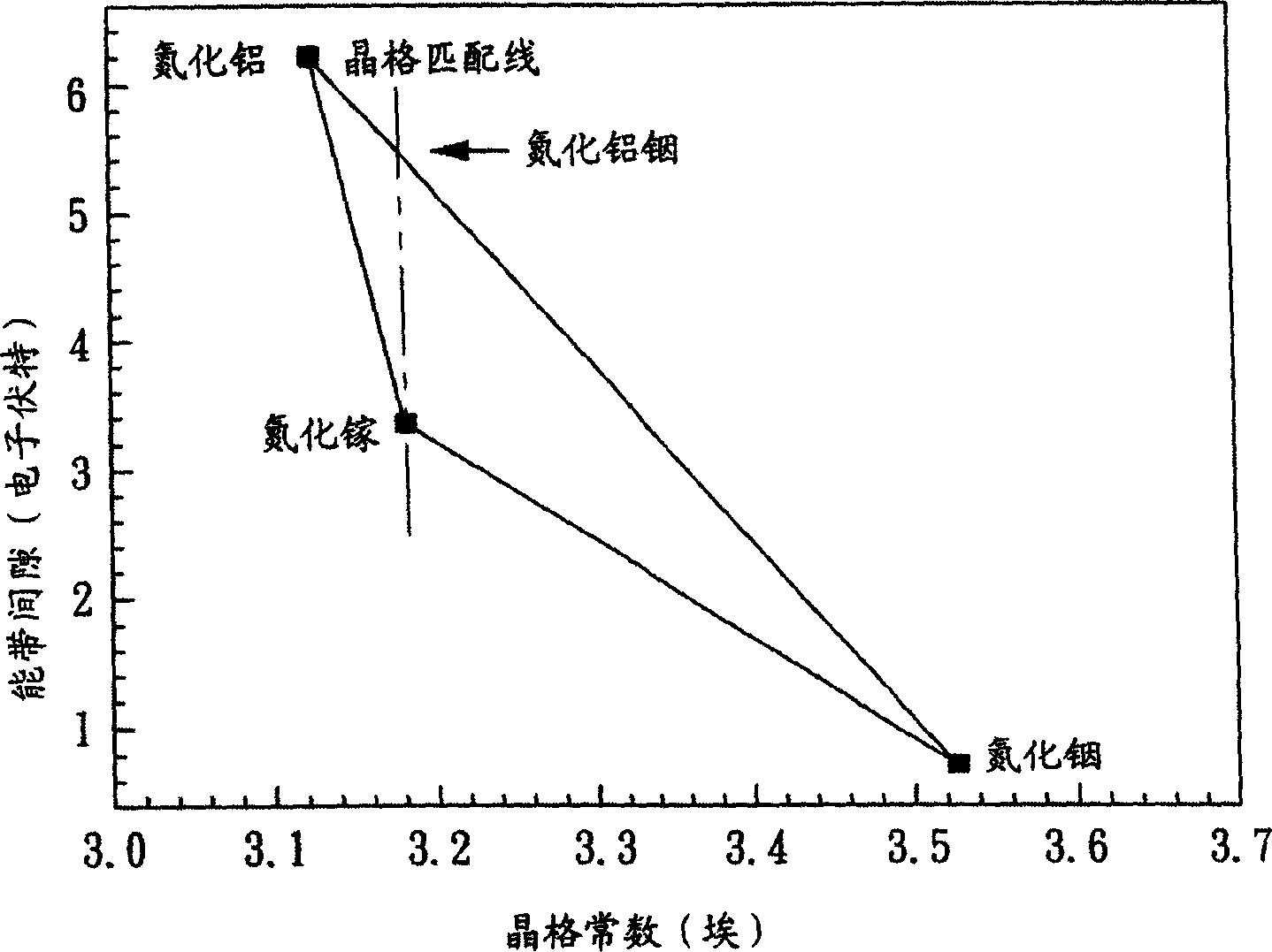
[0031] The substrate 11 is made of aluminum oxide single crystal (Sapphire). A buffer layer (buffer layer) 12 located on the substrate 11 is made of aluminum gallium indium nitride (AlGaN) 1-x-y Ga x In y N), wherein 0≤X1-x In x N), where 0≤X<1. The p-type cladding layer 15 has a thickness ranging from 50 angstroms to 3000 angstroms. The growth temperature of the p-type cladding layer 15 is between 600°C and 1200°C.
[0032] The contact layer 16 on the p-type cladding layer 15 is made of Mg-doped p-type gallium nitride (GaN).
[0033] The first embodiment of the GaN-based LED structure of the present invention may further include an electrode layer 17 located on th...
no. 4 example
[0044] The fourth embodiment of the gallium nitride-based light-emitting diode structure of the present invention includes: a substrate 41, a buffer layer 42, an n-type gallium nitride (GaN) layer 43, an active light-emitting layer 44, a double coating layer 45, and a contact layer 46 .
[0045] The substrate 41 is made of alumina single crystal. The buffer layer 42 on the substrate 41 is made of aluminum gallium indium nitride (AlGaN) 1-x-y Ga x In y N), wherein 0≤X1-x In x N), where 0≤X1-z In z N), where 0≤Z<1. The thickness of the second coating layer 452 is between 50 (Å) to 3000 (Å), and the growth temperature is between 600°C and 1200°C.
[0046] The contact layer located on the double coating layer 45 is made of magnesium (Mg) doped aluminum indium nitride (Al 1-x In x N) p-type gallium nitride (GaN), where 0≤X<1.
[0047] The fourth embodiment of the GaN-based LED structure of the present invention may further include an electrode layer 47 located on the conta...
PUM
 Abstract
Description
Claims
Application Information
 - R&D
- Intellectual Property
- Life Sciences
- Materials
- Tech Scout
- Unparalleled Data Quality
- Higher Quality Content
- 60% Fewer Hallucinations
Browse by: Latest US Patents, China's latest patents, Technical Efficacy Thesaurus, Application Domain, Technology Topic, Popular Technical Reports.
© 2025 PatSnap. All rights reserved.Legal|Privacy policy|Modern Slavery Act Transparency Statement|Sitemap|About US| Contact US: help@patsnap.com