

Fin field effect transistor memory cell, fin field effect transistor memory cell arrangement, and method for the production of a fin field effect transistor memory cell
A fin-type field effect and storage unit technology, which is applied in transistors, semiconductor/solid-state device manufacturing, information storage, etc., can solve the problems of low size application flexibility, high voltage, and low read current, and achieve the best size application effect
- Summary
- Abstract
- Description
- Claims
- Application Information
AI Technical Summary
Problems solved by technology
Method used
Image

Examples
Embodiment Construction
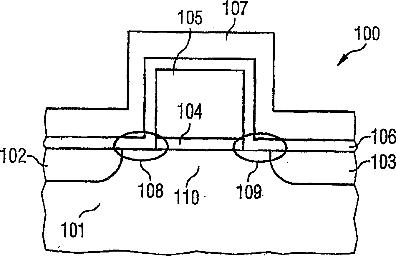
[0049] see figure 1 , which illustrates the way of performing source-side (or drain-side) charge carrier injection with a gate, wherein the gate is divided into a control gate and a word line, and is electrically decoupled from the latter; this The inventive memory cell can be programmed or read by the following programming methods.
[0050] figure 1 A memory cell 100 is illustrated, which is formed on and within a silicon substrate 101; the silicon substrate 101 has a gate dielectric 104 thereon, and is located between a first and a second bit line 102, 103 rooms. A control gate 105 is arranged on the gate dielectric 104, and an ONO layer sequence 106 is formed on this layer sequence as a charge storage layer. A word line 107 is formed on the ONO layer sequence 106 , and the word line 107 extends across the bit lines 102 , 103 and is electrically decoupled from the bit lines 102 , 103 by the ONO layer sequence 106 . also, figure 1 A first charge storage region 108 of the...
PUM
 Abstract
Description
Claims
Application Information