
B-ga2o3 single crystal growing method, thin-film single crystal growing method, ga2o3 light-emitting device, and its manufacturing method

A growth method, a technology for growing crystals, applied in the directions of single crystal growth, single crystal growth, crystal growth, etc., which can solve the problems of deterioration, target object degradation, and hindering the growth of thin film single crystals, etc.

Inactive Publication Date: 2006-03-29
WASEDA UNIV
View PDF4 Cites 56 Cited by
  • Summary
  • Abstract
  • Description
  • Claims
  • Application Information

AI Technical Summary

Problems solved by technology

In addition, since the target object is sometimes deteriorated or deteriorated due to laser irradiation, this becomes a factor hindering thin film single crystal growth

Method used


Image

  • B-ga2o3 single crystal growing method, thin-film single crystal growing method, ga2o3 light-emitting device, and its manufacturing method
  • B-ga2o3 single crystal growing method, thin-film single crystal growing method, ga2o3 light-emitting device, and its manufacturing method
  • B-ga2o3 single crystal growing method, thin-film single crystal growing method, ga2o3 light-emitting device, and its manufacturing method

Examples


no. 1 approach

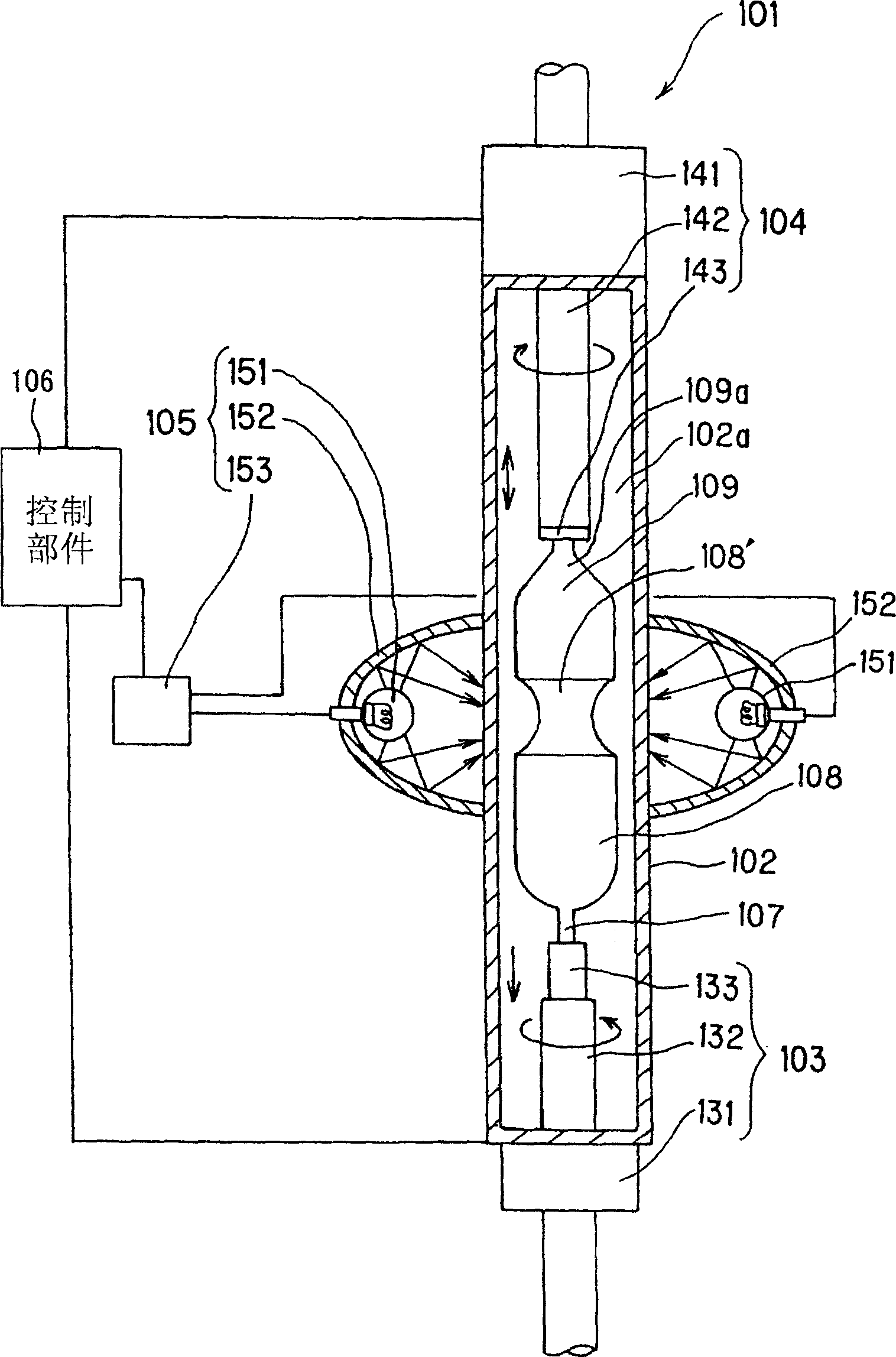
[0053] figure 1 An infrared heating single crystal manufacturing apparatus according to the first embodiment of the present invention is shown, in which the infrared heating single crystal manufacturing apparatus 101 is used to manufacture β-Ga according to the FZ method 2 o 3 single crystal, the device schematically consists of a silica tube 102 for clamping / rotating β-Ga 2 o 3 A seed crystal rotating part 103 of a seed crystal (hereinafter referred to as "seed crystal") 107 for clamping / rotating β-Ga 2 o 3 The raw material rotating part 104 of the polycrystalline raw material (hereinafter simply referred to as "polycrystalline raw material") 109, the heating part 105 for heating the polycrystalline raw material 109 to make it melt, the seed crystal rotating part 103 and the control raw material rotating part 104 and the heating part 105 The control unit 106.

[0054] The seed crystal rotating part 103 is provided with a seed chuck that holds the seed crystal 107, a low...

no. 2 approach

[0084] Figure 7 A schematic configuration of a film forming apparatus according to a second embodiment of the present invention is shown. A film forming apparatus 201 performs film formation according to the PLD method, which is provided with a chamber 202 including a space 220 that can be evacuated, a target table 205 provided in the chamber 202, a target table 203 held on the target table , a rotating mechanical device 211 provided outside the chamber 202 and rotating the target stage 205, a substrate holding member 207 provided inside the chamber 202 and holding the substrate 206, the substrate 206 can be accommodated in the substrate holding member A heater for heating to 1500° C., a radical injecting part 208 for injecting radicals into the chamber 202 through a pipe 202 a, a vacuum pump (not shown) for evacuating the space 220 through a pipe 202 b to evacuate the space 220 and a laser section 204 provided outside the chamber 202 and irradiating a laser beam as an excit...

no. 3 approach

[0096] Figure 8 A cross section of an MIS type light emitting device according to a third embodiment of the present invention is shown. The MIS type light emitting device 260 is provided with a β-Ga 2 o 3 Substrate 206 made of single crystal, β-Ga 2 o 3 Thin film single crystal 261, made of β-Ga 2 o 3 Thin film crystals are fabricated and formed on n-type β-Ga 2 o 3 The insulating layer 262 on the top of the thin film single crystal 261, the gold electrode 263 formed on the top of the insulating layer 262, the bonding material (bonding) 267 attached to the top of the gold electrode 263 and connected to the lead 268, the n-electrode 264 formed on the bottom of the substrate 206 and Bonding material 265 attached to the bottom of n-electrode 264 and connected to lead 266 .

[0097] By making β-Ga 2 o 3 Crystal annealing forms insulating layer 262 with no oxygen vacancies in the surface of 10-1000 nm.

[0098] According to a third embodiment, a light emitting device wi...


PUM

PropertyMeasurementUnit
Carrier concentrationaaaaaaaaaa

Abstract

PROBLEM TO BE SOLVED: To provide a method for growing a β-f-based single crystal which is less prone to be cracked even when it is worked into a large size and high quality substrate or the like. ŽSOLUTION: The β-Ga<SB>2< / SB>O<SB>3< / SB>single crystal 8 is allowed to grow in one orientation selected from a-axis <100> orientation, b-axis <010> orientation, and the orientation inclined by 13.7°, determined crystallographically, from c-axis toward a-axis and having an angle of 90° with respect to a-axis by heating a seed crystal 7 and a polycrystalline base material 9 while rotating the crystal 7 and the base material 9 mutually in the opposite directions by using an infrared heating single crystal manufacturing device 1. Ž

Description

[0001] The present invention is based on Japanese Patent Application No. 2003-46552, No. 2003-66020 and No. 2003-137916, the entire contents of which are incorporated herein by reference. field of invention [0002] The present invention relates to β-Ga 2 o 3 Single crystal growth method, thin film single crystal growth method, Ga 2 o 3 Light-emitting device and method of manufacturing the same, and more particularly, the present invention relates to growing β-Ga 2 o 3 The method of single crystal, the method of growing single crystal with high-quality thin film, Ga that can emit light in the ultraviolet region 2 o 3 Light emitting device and its manufacturing method. Background technique [0003] In the realization of mercury-free fluorescent lamps, photocatalysts that provide a clean atmosphere, next-generation DVDs that enable higher-density recording, and the like, light-emitting devices in the ultraviolet region are obviously particularly desired. In view of thes...

Claims


Application Information

Patent Timeline
IPC IPC(8): C30B29/16C30B13/24H01L33/00H01S5/323C01G15/00C30B13/00C30B13/34
Inventor 一之濑升岛村清史青木和夫恩卡纳西翁·安东尼亚·加西亚·比略拉
Owner WASEDA UNIV
Learn More