Apparatus for repairing circuit pattern and method for manufacturing display apparatus using the same

A technology of graphics and inspection devices, applied in nonlinear optics, instruments, optics, etc., to achieve the effects of improving display quality, improving correction accuracy, and shortening time

Inactive Publication Date: 2006-04-05
JAPAN DISPLAY INC
View PDF5 Cites 36 Cited by
  • Summary
  • Abstract
  • Description
  • Claims
  • Application Information

AI Technical Summary

Problems solved by technology

Therefore, it is desirable to be able to automatically determine the laser irradiation area

Method used


Image

  • Apparatus for repairing circuit pattern and method for manufacturing display apparatus using the same
  • Apparatus for repairing circuit pattern and method for manufacturing display apparatus using the same
  • Apparatus for repairing circuit pattern and method for manufacturing display apparatus using the same

Examples


Embodiment 1

[0077] Generally, a liquid crystal display device is a structure in which liquid crystal is sandwiched between two glass substrates, and the molecules of liquid crystal in each pixel are affected by the electric field in the capacitor formed by the pixel electrodes of multiple images arranged in a matrix, the opposite electrode and the liquid crystal. The orientation is controlled to generate an electronic latent image, and in a transmissive liquid crystal display device, the electronic latent image is visualized to display an image by controlling the transmittance of light from a backlight provided on the back. A color image is displayed by forming a circuit for controlling voltage applied to pixel electrodes on an active matrix substrate, and forming, for example, three-color color filters on a color filter substrate.

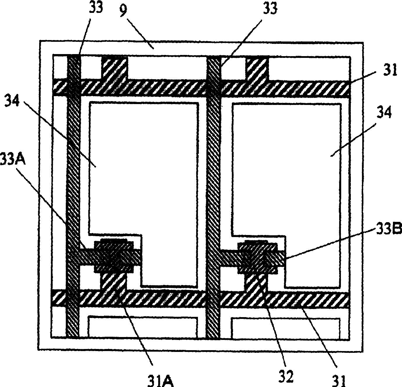
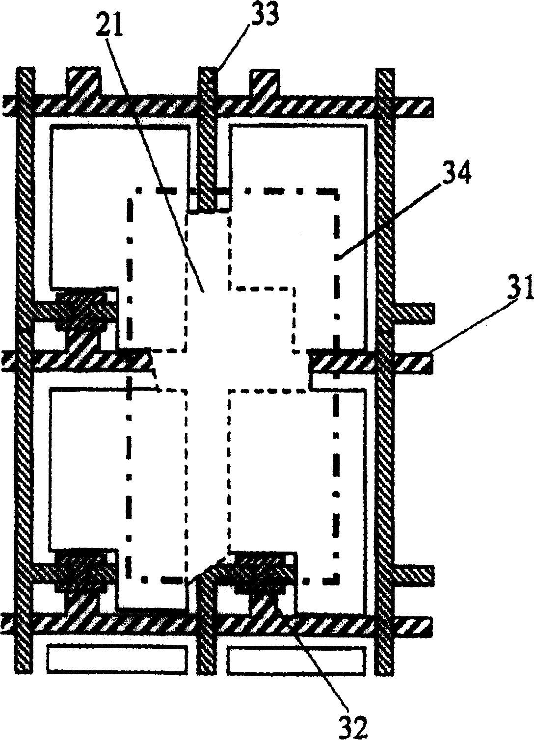
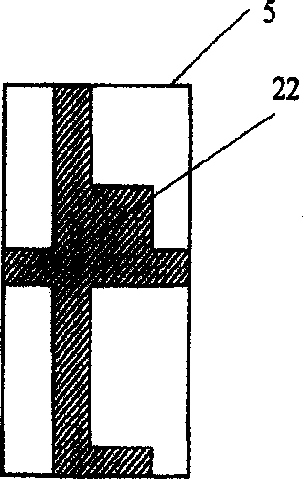
[0078] figure 1 This is a schematic plan view illustrating an example of pixels formed on an active matrix substrate of a liquid crystal display device. ex...

Embodiment 2

[0143] Figure 26 For illustrating the process diagram of embodiment 2 of the present invention. Figure 26 A manufacturing process of a glass substrate forming a switching element thin film transistor used in a liquid crystal panel in Example 2 is shown. The glass substrate on which this switching element is formed is generally referred to as a "TFT substrate" or "array substrate", and is hereinafter referred to as a TFT substrate. In Example 2, first, an inorganic film or an organic film is formed on a glass substrate provided when manufacturing a TFT substrate (S10).

[0144] A typical inorganic substance includes a metal material constituting the wiring of the TFT substrate. A photoresist is coated on the film-formed glass substrate and fired (S11).

[0145] Here, the so-called photoresist is a photosensitive material, which is used to process the film-forming material into a predetermined shape. Thereafter, by exposing the photoresist to light (S12), the photoresist i...

Embodiment 3

[0152] Figure 27 For illustrating the process diagram of embodiment 3 of the present invention. exist Figure 27 In , the manufacturing process of the TFT substrate used in the liquid crystal panel is shown. In Example 3, first, an inorganic film or an organic film is formed on a glass substrate provided when manufacturing a TFT substrate (S30). Here, since a transparent metal ITO (indium tin oxide) provided on a TFT substrate can be mentioned as a typical inorganic material for film formation, the following description will be made using an ITO film as a representative example.

[0153] At the stage where film formation is completed, visual inspection is performed (S31). Here, since ITO is transparent, it can be seen that there are foreign matter on ITO and foreign matter in the lower layer of ITO. The results of the visual inspection at the film formation completion stage are accumulated in the process of depositing the visual inspection results after film formation ( S...


PUM


Abstract

The invention relates to a manufacturing method of a graph amendment device and a display device. Pixels are arranged in the area which is enclosed with two grid wirings and two leakage wirings; as to the short-circuit defect of an adjacent pixel electrode, a laser exposure is caused to eliminate the short-circuit part through the mask of a transmission graph which corresponds to the grid wiring and leakage wiring of the short-circuit part and the graph of the pixel electrode. The elimination of the short-circuit part can be known by utilizing the information sent out by an inspection device to be compared with the normal graph, and the graph defect formed on a substrate can be automatically amended. Thus, the display device with a high-quality absorption characteristic can be realized by causing the method to be applied to the manufacturing process of the display device, in particular to the photoresist graph forming process.

Description

technical field [0001] The present invention relates to the method of correcting the convex part of the pattern shape of the substrate forming the predetermined pattern by using laser light, and correcting the missing part by applying wiring material graphic correction The technology is applicable to a method of manufacturing a liquid crystal display device. In addition, the present invention relates to a technology for manufacturing a display device, and particularly relates to a technology for preventing the occurrence of defective circuit patterns produced on a TFT substrate or the like. Background technique [0002] A liquid crystal display device is a structure in which liquid crystal is sandwiched between two glass substrates, and resins (colored resins) that are alternately coated with blue, green, and red are formed on a glass substrate (also called a color filter (CF) substrate). On another substrate (also known as an active matrix substrate or thin film transistor...

Claims


Application Information

Patent Timeline
Patent Type & Authority Applications(China)
IPC IPC(8): G02F1/13G02F1/1333
Inventor 中须信昭山田薰田中雄一郎新井武朴木秀行吉村和士川村彻也大川政德
Owner JAPAN DISPLAY INC
Why Eureka
Try Eureka