Face-down bonding structure with low-melting point convex point and making method
A technology of flip-chip welding and manufacturing methods, which is applied in semiconductor/solid-state device manufacturing, electrical components, electric solid-state devices, etc., and can solve problems such as enlarged bump area of flip-chip soldering, damage to ultrasonic power devices, and high melting point of electrodes, achieving Good adhesion, reduced device damage, lower melting point
- Summary
- Abstract
- Description
- Claims
- Application Information
AI Technical Summary
Problems solved by technology
Method used
Image


Examples
Embodiment 1
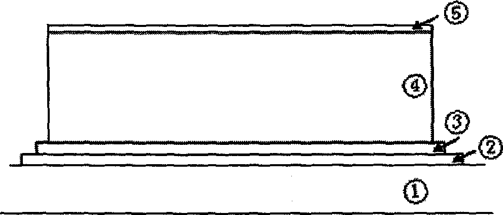
[0071] Side view of bump structure see image 3 , in the figure, the bump 4 is covered with a layer of Au / Sn alloy layer 5 or other low melting point alloy layer such as Pb / Sn, with a thickness of 0.01 μm. The Au / Sn alloy layer 5 can be formed by an evaporation process or a sputtering process. See the side view of the pad structure corresponding to the bump figure 2 .
Embodiment 2
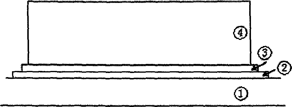
[0073] The side view of the bump structure see figure 1 . See the side view of the pad structure corresponding to the bump Figure 4 , in the figure, the pad 7 is covered with a layer of Au / Sn alloy layer 5 or other low melting point alloy layer such as Pb / Sn, with a thickness of 0.01 μm. The Au / Sn alloy layer 5 may be formed by an evaporation process or by a sputtering process.
Embodiment 3
[0075] Side view of bump structure see image 3 , in the figure, the bump 4 is covered with a layer of Au / Sn alloy layer 5 or other low melting point alloy layer such as Pb / Sn, with a thickness of 0.01 μm. The Au / Sn alloy layer 5 can be formed by an evaporation process or a sputtering process. See the side view of the pad structure corresponding to the bump Figure 4 In the figure, the pad 7 is also covered with a layer of Au / Sn alloy layer 5 or other low melting point alloy layer such as Pb / Sn, with a thickness of 0.01 μm. The Au / Sn alloy layer 5 may be formed by an evaporation process or by a sputtering process.
[0076] A specific manufacturing method of the pad electrodes and bumps capable of realizing the flip-chip bonding structure of the present invention will be described in detail below.
[0077] 1. Bumping process
[0078] 1. Fabrication of n-electrode insulating layer on silicon substrate
[0079] (1) Deposition of 0.3 μm thick SiO on the silicon substrate 2 ;...
PUM
| Property | Measurement | Unit |
|---|---|---|
| Height | aaaaa | aaaaa |
| Diameter | aaaaa | aaaaa |
| Height | aaaaa | aaaaa |
Abstract
Description
Claims
Application Information
 - Generate Ideas
- Intellectual Property
- Life Sciences
- Materials
- Tech Scout
- Unparalleled Data Quality
- Higher Quality Content
- 60% Fewer Hallucinations
Browse by: Latest US Patents, China's latest patents, Technical Efficacy Thesaurus, Application Domain, Technology Topic, Popular Technical Reports.
© 2025 PatSnap. All rights reserved.Legal|Privacy policy|Modern Slavery Act Transparency Statement|Sitemap|About US| Contact US: help@patsnap.com