Micro band slot array antenna

A microstrip slot and array antenna technology, which is applied in the direction of slot antennas, antennas, antenna arrays, etc., can solve the problems of large antenna thickness, low-profile advantages of microstrip antennas, and poor radiation performance.

Inactive Publication Date: 2006-06-14
上海联能科技有限公司 +1
View PDF0 Cites 17 Cited by
  • Summary
  • Abstract
  • Description
  • Claims
  • Application Information

AI Technical Summary

Problems solved by technology

In this way, the thickness of the entire antenna is relatively large, which greatly reduces the advantages of the low profile of the microstrip antenna.
In addition, since the slot and the reflective backplane are similar to a parallel plate waveguide, surface waves are easily e

Method used


Image

  • Micro band slot array antenna
  • Micro band slot array antenna
  • Micro band slot array antenna

Examples


Embodiment 1

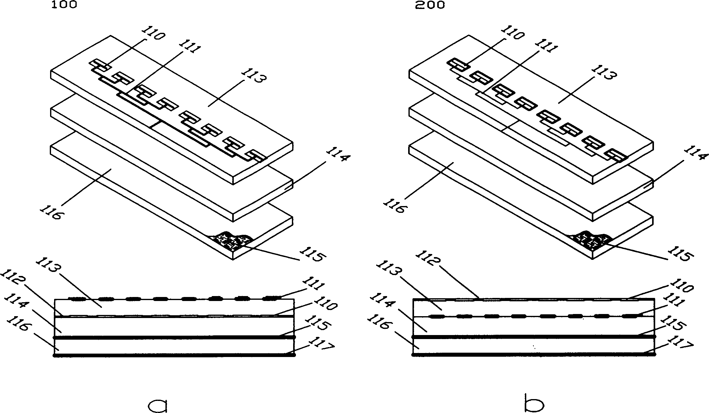
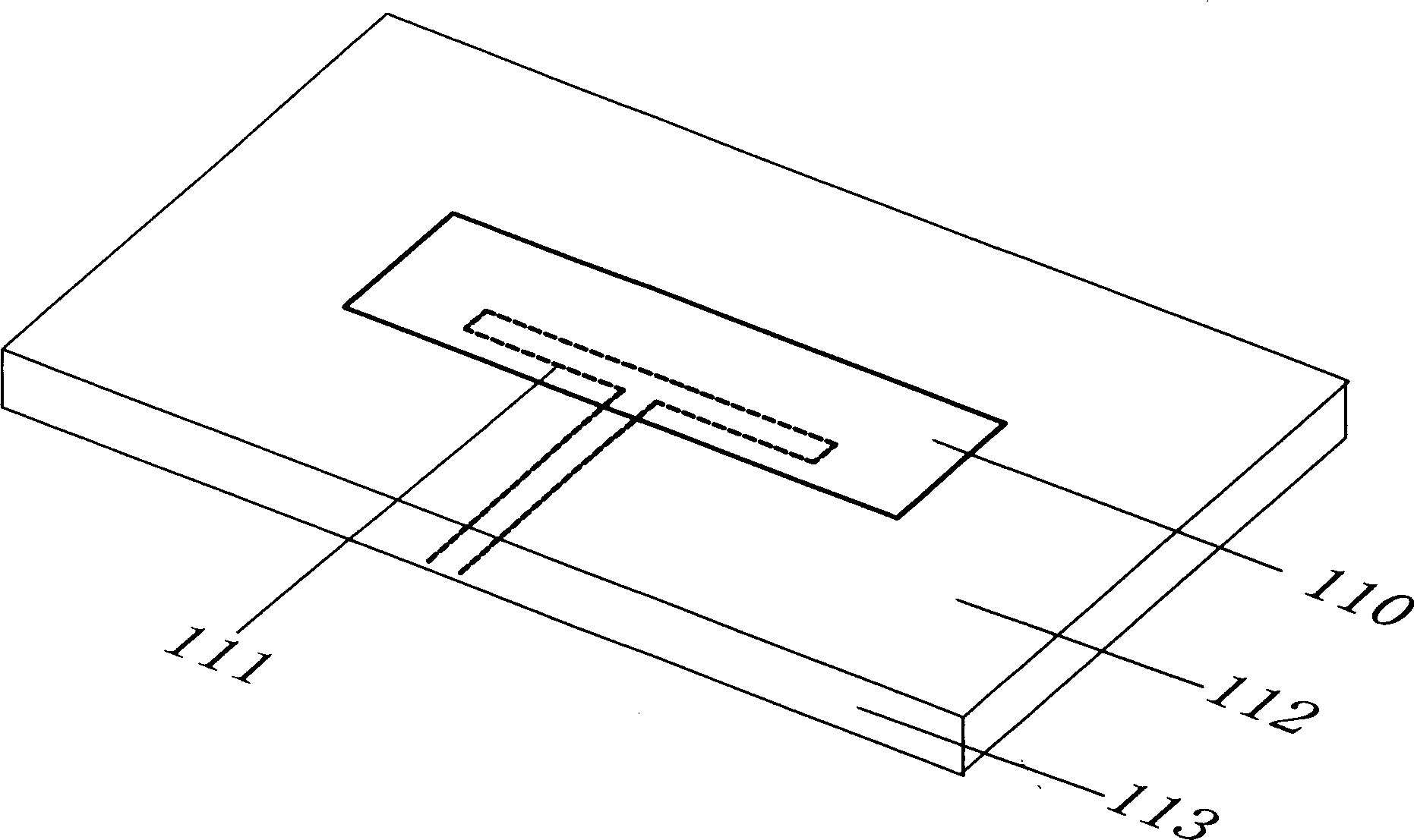
[0011] Example one, see figure 1 (a) This embodiment is a 1×8 matrix microstrip slot array antenna 100 with 8 slot antennas, the slot 110 is located on the lower surface of the dielectric plate 113, the periphery of the slot 110 is a metal ground 112, and the feed line 111 is located on the dielectric plate On the upper surface of 113, under the dielectric plate 113 is the isolation layer 114, and the bottom is the high-resistance magnetic permeable surface substrate 116. The high-resistance surface permeable pattern 115 is located on the upper surface of the high-resistance permeable surface substrate 116. The lower surface of is the metal base plate 117; the specific size parameters and material selection are calculated according to the applied frequency band according to the existing wireless communication theory. In this embodiment, the frequency application range is 3.4 GHz to 3.53 GHz, and the dielectric plate 113 is selected Microwave dielectric materials with a dielectric...

Embodiment 2

[0013] Example two, see figure 1 (b) This embodiment is a 1×8 matrix microstrip slot array antenna 200 with 8 slot antennas, the slot 110 is located on the upper surface of the dielectric plate 113, the periphery of the slot 110 is a metal ground 112, and the feed line 111 is located on the dielectric plate The bottom surface of 113, under the dielectric plate 113 is the isolation layer 114, the bottom is the high-resistance permeable surface substrate 116, the high-resistance surface permeable pattern 115 is located on the upper surface of the high-resistance permeable surface substrate 116, The lower surface of is the metal bottom plate 117; the specific size parameters and material selection are calculated according to the applied frequency band according to the existing wireless communication theory. In this embodiment, the frequency application range is 3.4 GHz to 3.53 GHz, and the dielectric plate 213 is selected Microwave dielectric materials with a dielectric constant of ...


PUM

PropertyMeasurementUnit
Lengthaaaaaaaaaa
Thicknessaaaaaaaaaa

Abstract

The invention provides a thinner, lighter, lower-bypass level plate-type micro band gap array antenna, replacing routine all metal guide face with fine-new artificial high impedance magnetic conduction face as a reflection back plate of the antenna array, able to reduce the space between the back plate and the gap array face from lambda/4 or 3 lambda/4 down to lambda/10 below (the desired space is zero), thus largely reducing the thickness of the antenna. Because foam medium is ordinarily filled between the back plate and the gap array face to support and isolate, the reduction of the space largely reduces the use quantity of the needed foam medium, thus largely reducing the large-scale antenna weight. Simultaneously, because the new magnetic conduction back plate has special electromagnetic band gap property, it can prohibit the propagation of surface wave and parallel plate mode electromagnetic wave, thus effectively reducing the bypass level of the antenna array. The artificial high impedance magnetic conduction face can be applied to various antenna arrays, such as 1x8, 2x8, 4x4, and other arrays.

Description

Technical field [0001] The invention relates to a microstrip slot array antenna, in particular to a flat microstrip slot array antenna using a brand-new artificial high-impedance magnetic guide surface as the reflection back plate of the antenna array. Background technique [0002] The microstrip antenna has the advantages of thin profile, small size, light weight, easy to form a conformal structure with the surface of the carrier, mass production with conventional printed circuit technology, low manufacturing cost, and easy integration with other solid-state microwave components. It is used in military and The field of civil communications has been widely used. In terms of specific structure, it can be subdivided into patch antennas, slot antennas, wire antennas, and dipole antennas. Compared with microstrip patch antennas and wire antennas, microstrip slot antennas have a higher frequency bandwidth. , Which can meet the frequency bandwidth requirements of most applications, and...

Claims


Application Information

Patent Timeline
IPC IPC(8): H01Q1/38H01Q13/10H01Q21/00
Inventor 贺连星刘晓晗殷杰羿资剑李毅丁振宇
Owner 上海联能科技有限公司
Why Eureka
Try Eureka