Multiplex test method for semiconductor wafer and multiplex test probe station therefor

A technology of testing probes and testing methods, which is applied in the direction of semiconductor/solid-state device testing/measurement, single semiconductor device testing, electrical measurement, etc., can solve the problems of slow speed and low efficiency, and achieve the effect of improving test speed and efficiency

Active Publication Date: 2006-06-21
SHENZHEN SIDEA SEMICON EQUIP
View PDF0 Cites 34 Cited by
  • Summary
  • Abstract
  • Description
  • Claims
  • Application Information

AI Technical Summary

Problems solved by technology

[0008] Since the probe station only completes the test of one chip every time it moves, there are problems of slow speed and low efficiency

Method used


Image

  • Multiplex test method for semiconductor wafer and multiplex test probe station therefor
  • Multiplex test method for semiconductor wafer and multiplex test probe station therefor

Examples


Embodiment Construction

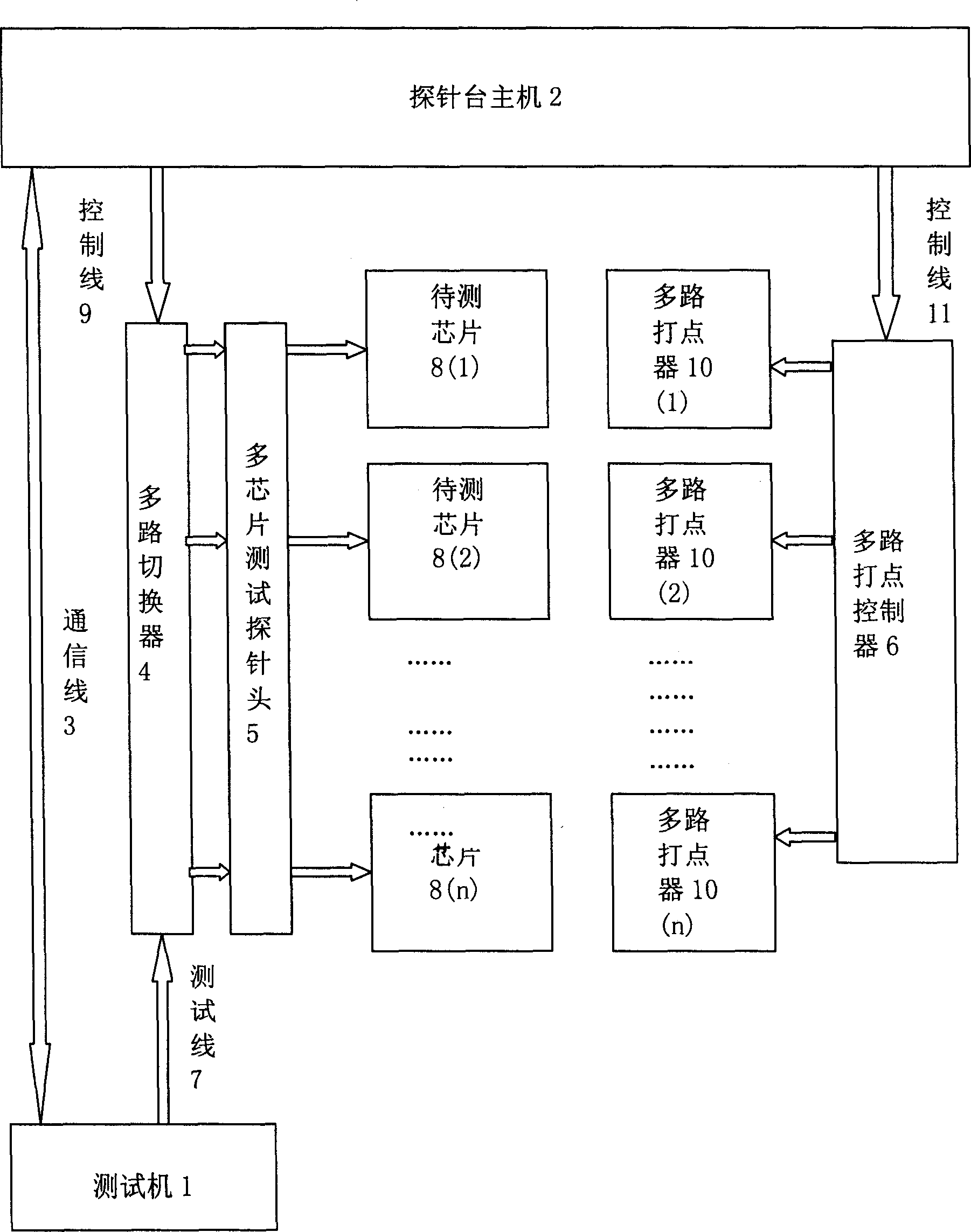
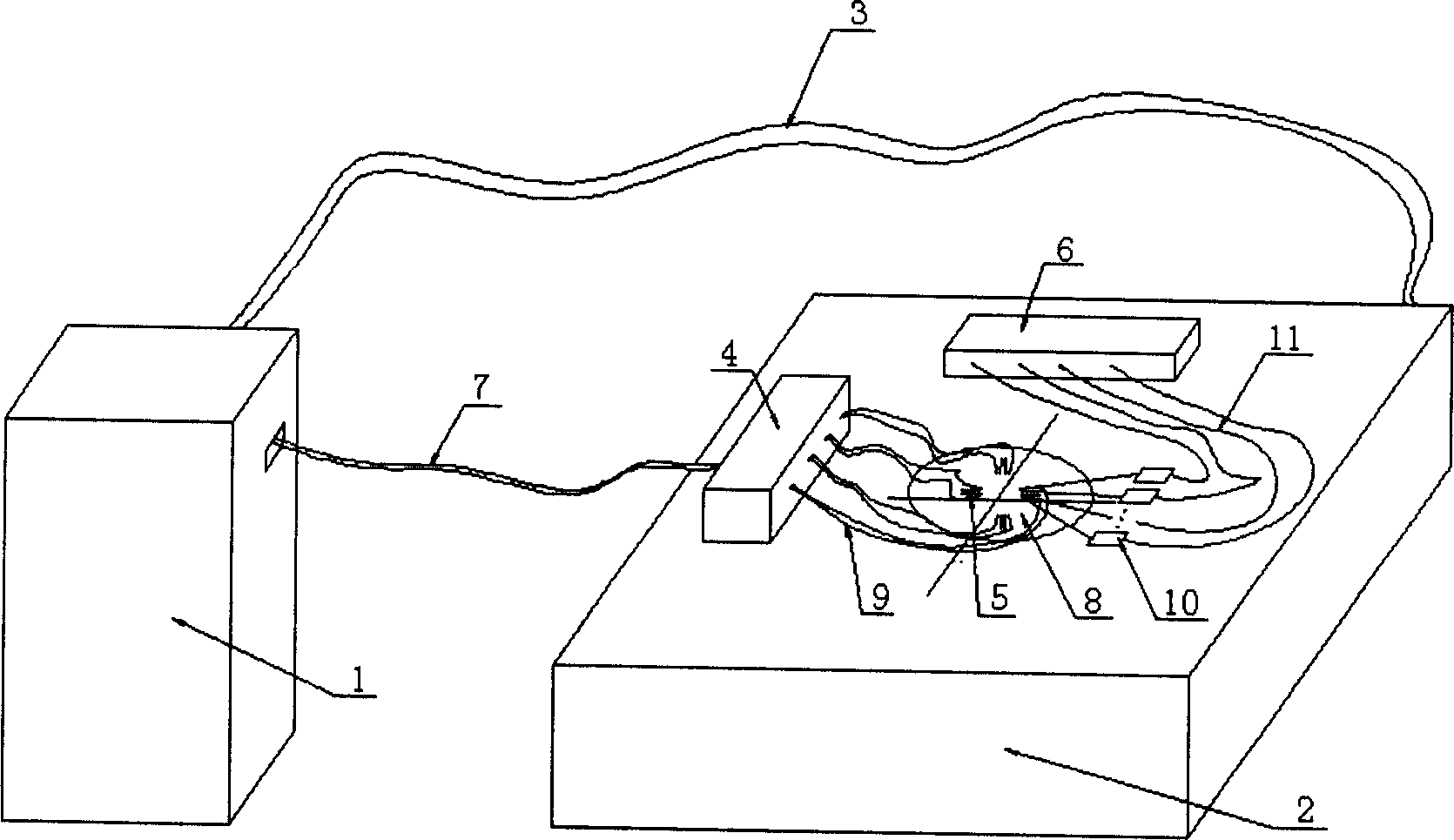
[0045] A multi-channel test probe station for triode wafer testing

[0046] Such as figure 1 , 2 The shown multi-channel test probe station includes a probe station host 2 embedded with multi-channel test and communication software, a multi-chip test probe head 5 fixedly arranged on the probe station host 2, and a multi-channel RBI controller 6 And the multi-channel dotting device 10 controlled by it, the multi-chip test probe head 5 is connected with the test line 7 drawn by the external testing machine 1 through the multiplexer 4, and the multi-chip test probe head 5 is provided with Multiple sets of test probes that can be connected to multiple chips at the same time.

[0047] The multi-way dotting device 10 is a multi-way marking device with the same number of test probes as the multi-chip test probe head 5. The multi-way dotting controller 6 is directly connected with the probe station host 2 through the control line 11. The needle table host 2 controls to mark the ink...


PUM


Abstract

The invention discloses a multipath detecting method of semi-conductor crystal disk with probe table host controlling the multipath switching device to make the detector of detecting set connecting each group of detecting probe. The multipath detecting probe table is characterized by the following: the multipath test and communication software are inserted in the host of probe table; the test probe is chip test probe with multipath test probe connecting multiple chips simultaneously; the marking device is multipath marking device, which marks the irregular chip controlled by probe table host; the quantity of multipath switching device is the same as the test probe of multichip test probe; the multipath switching device connects the test probe through the other control line, which connects the test probe with each corresponding a group of test probe of multichip test probe separately. The invention can finish testing at least two detected semiconductor chips in one moving period, which improves the test speed and efficiency greatly.

Description

technical field [0001] The invention relates to semiconductor wafer testing, in particular to a semiconductor wafer multi-channel testing method and a multi-channel testing probe station. Background technique [0002] The purpose of semiconductor wafer testing is to pick out defective chips in silicon wafers. At present, the multi-channel test technology controlled by the testing machine is widely used. It uses the probe station as the precise positioning unit, and the internal relay is controlled by the testing machine to switch to different semiconductor chips to be tested. The method is to follow the steps in sequence: [0003] (1) placing a silicon wafer composed of multiple chips on the probe station; [0004] (2) The probe station is positioned under the semiconductor chip to be tested by the XY motion platform controlled by the motor, and then the Z-direction lifting mechanism is controlled by the motor to lift the wafer upward, so that the semiconductor chip to be t...

Claims


Application Information

Patent Timeline
Patent Type & Authority Applications(China)
IPC IPC(8): G01R1/073G01R31/26H01L21/66
Inventor 杨波
Owner SHENZHEN SIDEA SEMICON EQUIP
Why Eureka
Try Eureka