

Negative nano-imprinting method
A nano-imprinting and negative-type technology, which is applied in the manufacture of electrical components, semiconductor/solid-state devices, circuits, etc., can solve problems such as easy-to-produce defects, and achieve the effects of easy control, avoiding stripping process, and low price
- Summary
- Abstract
- Description
- Claims
- Application Information
AI Technical Summary
Problems solved by technology
Method used
Image

Examples
Embodiment 1
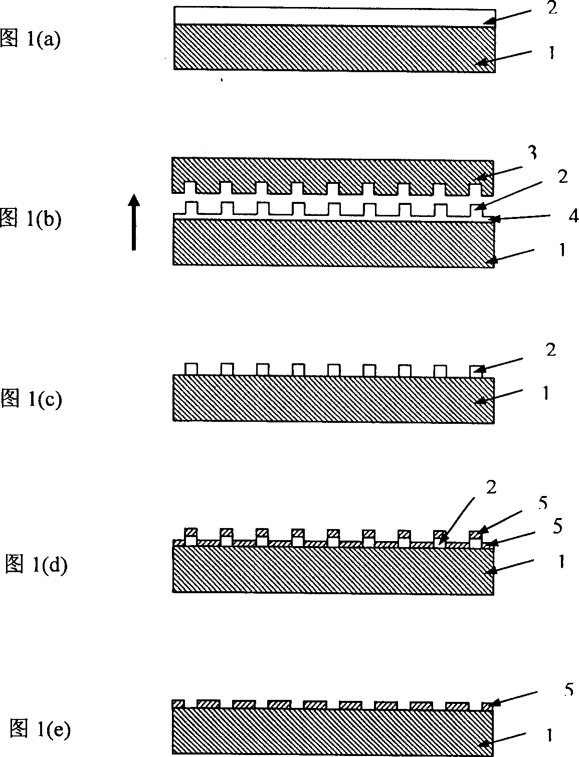
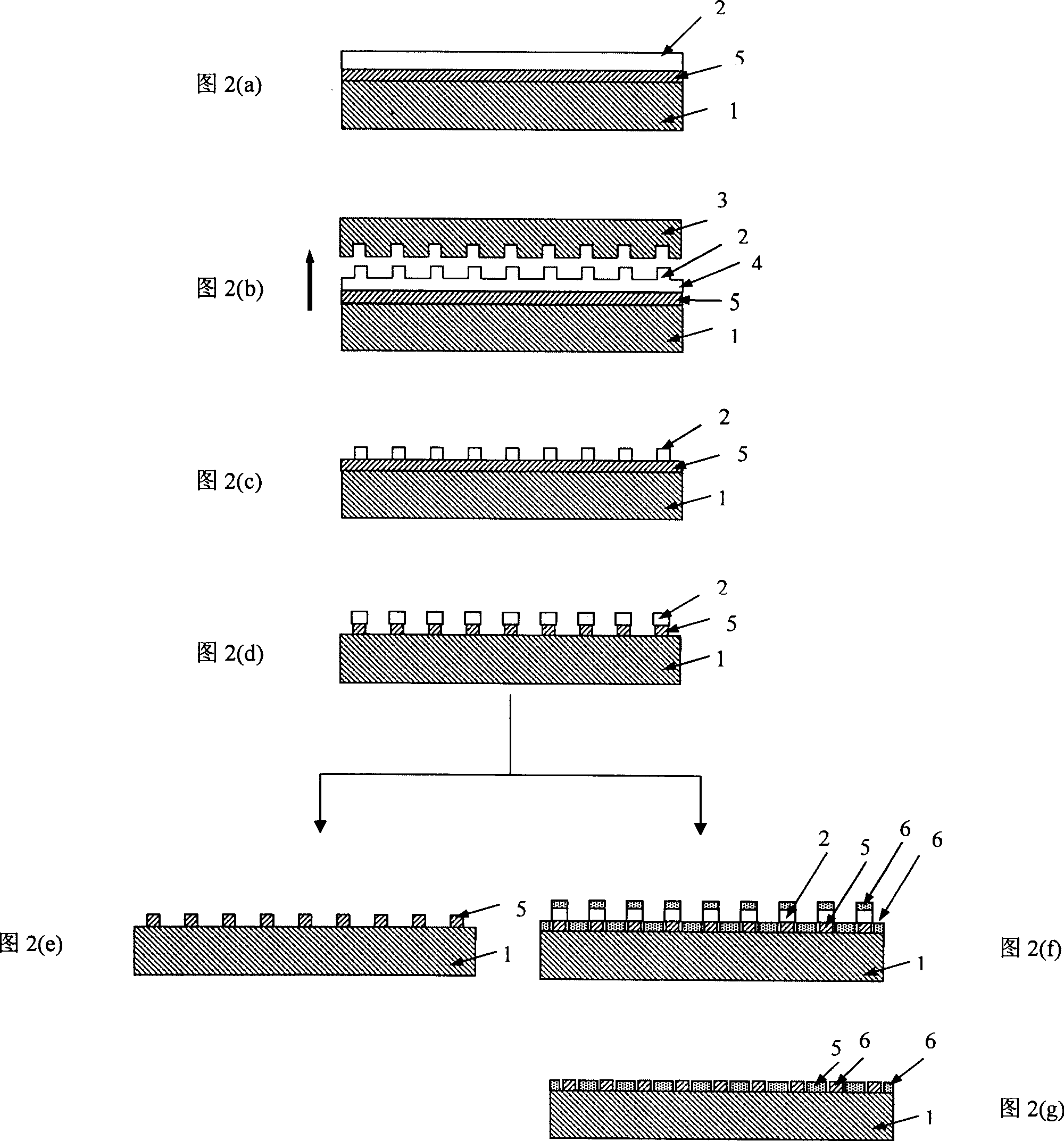
[0032] Embodiment 1: a kind of negative type nano imprinting method is characterized in that it is made of following steps (see figure 2 ): (1) first vapor-deposit metal film layer 15 on silicon substrate 1, and spin-coat photoresist 2 on metal film layer 15 (see figure 2 -a); (2) the nano-pattern of the template 3 is copied to the photoresist 2 under heat and pressure conditions (see figure 2 -b), (3) and transfer the pattern to the metallized film layer I5 with reactive ion etching technology (see figure 2 -c); (4) then use the pattern of photoresist 2 as a mask to etch the bare metal I5 that is not covered by photoresist 2 (see figure 2 -d); (5) making metal nanostructures.
[0033]The metal nanostructure that above-mentioned step (5) makes obtains single metal nanostructure by directly dissolving photoresist 2 with organic solvent (see figure 2 -e).
Embodiment 2
[0034] Embodiment 2: a kind of negative type nano imprinting method is characterized in that it is made of following steps (see figure 2 ): (1) first vapor-deposit metal film layer 15 on silicon substrate 1, and spin-coat photoresist 2 on metal film layer 15 (see figure 2 -a); (2) the nano-pattern of the template 3 is copied to the photoresist 2 under heat and pressure conditions (see figure 2 -b), (3) and transfer the pattern to the metallized film layer I5 with reactive ion etching technology (see figure 2 -c); (4) then use the pattern of photoresist 2 as a mask to etch the bare metal I5 that is not covered by photoresist 2 (see figure 2 -d); (5) making metal nanostructures.
[0035] The metal nanostructure that above-mentioned step (5) makes is by using the pattern of photoresist 2 as mask evaporation metal II6 (see figure 2 -f), then remove the photoresist 2 with an organic solvent to prepare a double metal nanostructure (see figure 2 -g).
Embodiment 3
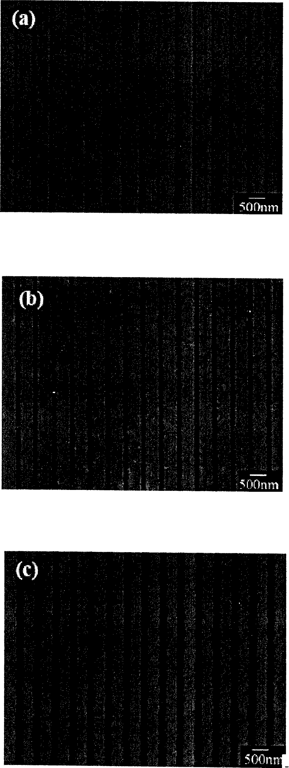
[0036] Example 3: Preparation of SiO by Combining Direct Write Electrotechnical Beam Exposure Technology and Reactive Ion Etching Technology 2 / Si template, the line width, period and height of the template pattern are 170nm, 370nm and 130nm respectively. Take a 2×2cm silicon wafer, after cleaning, vapor-deposit a 25nm thick gold film, then spin-coat photoresist on the surface of the gold film, dry it at 170°C, and the thickness will be 150nm, and then copy the nanometer pattern on the template to the On photoresist (imprint conditions: 190°C, 45bar, 3min). The redundant photoresist in the groove is removed by reactive ion etching process, and the nanometer pattern is transferred to the surface of the gold film. Then use the photoresist nanopattern as a mask, and use KI / I 2 solution (0.0025M I 2 +0.015M KI) to dissolve the exposed gold film for 40s, and then remove the photoresist with hot acetone under ultrasonic conditions to obtain a gold nanostructure with a line width ...
PUM
 Abstract
Description
Claims
Application Information