Small-sized on-chip CMOS power amplifier having improved efficiency

A power amplifier and amplifier technology, applied in the field of radio frequency systems, can solve problems such as performance deterioration, power amplifier efficiency reduction, and secondary coil quality factor reduction.

Inactive Publication Date: 2006-07-12
SAMSUNG ELECTRONICS CO LTD
View PDF2 Cites 9 Cited by
  • Summary
  • Abstract
  • Description
  • Claims
  • Application Information

AI Technical Summary

Problems solved by technology

However, since the value of the K factor (coupling coefficient) is in the range of 0.5 to 0.6, the Figure 4 The power amplifier shown in the reduced efficiency
In addition, the quality factor Q2 of the secondary coil must be reduced according to the impedance transformation ratio
[0012] also, Figure 4 The power amplifier shown in has current crowding effects and an unbalanced input signal due to input feeder coupling, resulting in severe performance degradation

Method used


Image

  • Small-sized on-chip CMOS power amplifier having improved efficiency
  • Small-sized on-chip CMOS power amplifier having improved efficiency
  • Small-sized on-chip CMOS power amplifier having improved efficiency

Examples


Embodiment Construction

[0034] Hereinafter, preferred embodiments of the present invention will be described in detail with reference to the accompanying drawings. It should be noted that identical or similar elements in the drawings are denoted by the same reference numerals as much as possible even though they are shown in different drawings. Also, in the following description of the present invention, when a detailed description of known functions and configurations incorporated herein may make the subject matter of the present invention unclear, it will be omitted.

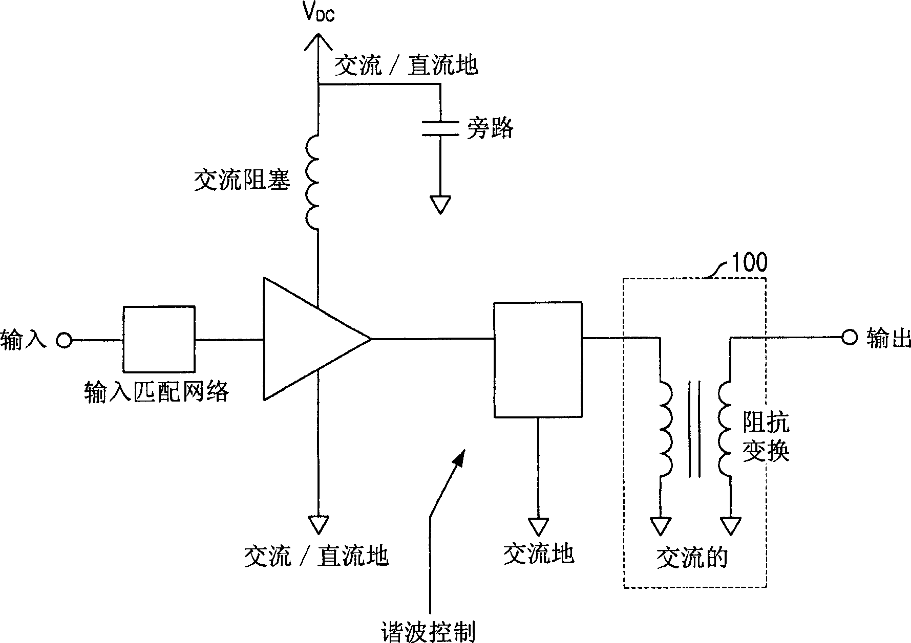
[0035] Figure 5A to Figure 5C is a diagram showing a small-sized on-chip CMOS power amplifier with improved efficiency according to an embodiment of the present invention. more specifically, Figure 5A to Figure 5C Shown is a small-sized on-chip CMOS power amplifier with improved efficiency, in which a distributed active converter ( The position of the primary coil and the secondary coil of DAT) can easily realize the optimized Q...


PUM


Abstract

The present invention provides a small-sized on-chip complementary metal oxide semiconductor (CMOS) power amplifier with improved efficiency. The on-chip CMOS power amplifier can improve efficiency and maximize its output by increasing the K factor, which can cause problems in power amplifiers with distributed active converter structures. The on-chip CMOS power amplifier, which has improved efficiency and is manufactured in a small size, includes: a primary coil, located in the first layer; a secondary coil, located in the second layer, the second layer being the upper part of the first layer, the secondary coil corresponding Placed at the position of the primary coil; the cross section is used to couple the secondary coils to each other.

Description

technical field [0001] The present invention relates generally to radio frequency (RF) systems, and more particularly to the integration of power amplifier sections for RF systems. Background technique [0002] Recently, the trend of radio frequency (RF) systems focuses on "RF systems on a chip". Therefore, Monolithic Microwave Integrated Circuit (MMIC) technology and Complementary Metal Oxide Semiconductor (CMOS) technology have attracted attention. MMIC technology enables passive components such as resistors, inductors, and capacitors and active components such as transistors and field effect transistors (FETs) to be fabricated on one semiconductor substrate through an integrated process, and CMOS technology enables all logic circuits and all high-frequency RF analog circuits are implemented on a chip at low cost. In particular, although CMOS technology may be determined as the ultimate technology in which all logic circuits and all high-frequenc...

Claims


Application Information

Patent Timeline
Patent Type & Authority Applications(China)
IPC IPC(8): H03F1/02H03F3/21H03F3/60
CPCE04H12/08E04H12/12
Inventor 李在燮姜贤一李成洙赫格·罗萨高柱泫白东铉洪圣喆
Owner SAMSUNG ELECTRONICS CO LTD
Why Eureka
Try Eureka