Adhesion method using gray-scale photolithography

A technique of grayscale, composition, applied in the direction of originals for photomechanical processing, microlithography exposure equipment, optics, etc.

Inactive Publication Date: 2006-07-26
DOW CORNING CORP
View PDF20 Cites 3 Cited by
  • Summary
  • Abstract
  • Description
  • Claims
  • Application Information

AI Technical Summary

Problems solved by technology

These defects can occur in any of several steps in conventional photolithography

Method used


Image

  • Adhesion method using gray-scale photolithography
  • Adhesion method using gray-scale photolithography

Examples


Embodiment 1

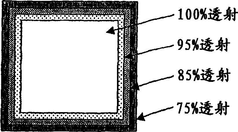
[0108] Repeat Comparative Example 1, except that a standard photomask is used and a grayscale binary photomask is used. The grayscale binary photomask is designed so that the perimeter of the pad receives a reduced amount of radiation during the photolithography process. More specifically, the photomask defines a 5 x 5mm pad as a series of squares whose transmittance drops from 100% to 75%, with each additional square falling in intensity, as figure 1 shown. From 95% to 75% of the intensity is in the 50 micron band, and the intensity in each band is controlled by pixels with a size of 0.5 micron. The intensity was adjusted between the bands by increasing the number of opaque 1 micron pixels randomly placed on each band.

[0109] Compared to Comparative Example 1, the resulting patterned film (ie, mat) has reduced surface non-uniformity (reduced side peaks). Interfacial contact is greater than 80%. Die shear value greater than 20kg.

Embodiment 2

[0112] Comparative Example 2 was repeated, except that a grayscale photomask designed so that the periphery of the pads received a reduced amount of radiation during photolithography was used as in Example 1 . Compared to Comparative Example 2, the resulting patterned film (ie, mat) had reduced surface non-uniformity (reduced side peaks). Interfacial contact is greater than 80%. Die shear value greater than 20kg.

Attached picture

[0113] figure 1 is the grayscale photomask used in Examples 1 and 2 of the present invention.

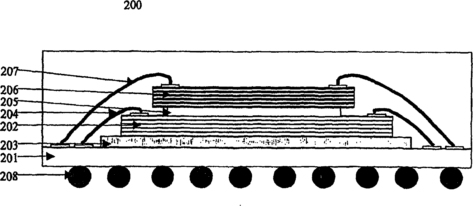
[0114] figure 2 It is a device manufactured by the method of the present invention.


PUM

PropertyMeasurementUnit
wavelengthaaaaaaaaaa
particle sizeaaaaaaaaaa
thicknessaaaaaaaaaa

Abstract

A method for adhering substrates using gray-scale photolithography includes: (a) applying a photopatternable corn-position to a surface of a substrate to form a film; (b) exposing a portion of the film to radiation having a wavelength of from 150 to 800 nm through a gray-scale photomask to produce an exposed film having non-exposed regions covering at least a portion of the surface; (c) heating the exposed film for an amount of time such that the exposed regions are substantially insoluble in a developing solvent and the nonexposed regions are soluble in the developing solvent; (d) removing the non-exposed regions of the heated film with the developing solvent to form a patterned film; (e) heating the patterned film for an amount of time sufficient to form a cured patterned film having a surface; (f) activating the surface of the cured patterned film and a surface of an adherend; (g) contacting the activated surface of the cured patterned film with the activated surface of the adherend. The photopatternable composition includes: (A) an organopolysiloxane containing an average of at least two silicon-bonded unsaturated organic groups per molecule, (B) an organosilicon compound containing an average of at least two silicon-bonded hydrogen atoms per molecule in a concentration sufficient to cure the composition, and (C) a catalytic amount of a photoactivated hydrosilylation catalyst.

Description

[0001] cross reference [0001] This application claims priority under 35 U.S.C. 119(e) to U.S. Provisional Application Serial No. 60 / 480641, filed June 23, 2003. US Provisional Application Serial No. 60 / 480641 is hereby incorporated by reference. technical field [0002] The present invention relates to methods of improving adhesion using photolithography to produce smooth surface films. The method may include plasma treating the film and the adherend bonded to the film to further improve adhesion. This method can be used in electronic packaging applications. Background technique [0003] Photolithography is a technique in which a substrate is covered with a photopatternable composition that is a radiation sensitive material. The film is selectively exposed to radiation, ie a portion of the film is exposed to radiation while another portion remains unexposed. Selective exposure of the film can be performed by placing a photomask between the radiation source and the film...

Claims


Application Information

Patent Timeline
Patent Type & Authority Applications(China)
IPC IPC(8): G03F7/075G03F1/00G03F7/20G03F7/40H01L21/58H01L21/98
CPCH01L2924/01043H01L2924/0105H01L2924/01041H01L2924/01045H01L2224/32014H01L2224/8301G03F7/201H01L2924/15311H01L23/3128H01L2924/01044H01L2224/29355H01L2224/29H01L2224/48091H01L2924/01013H01L2924/01003H01L2224/32225H01L2224/29298H01L2924/0665H01L25/50H01L2924/0103H01L2224/2919H01L2224/2929H01L2924/01068H01L2924/0104H01L2924/01076H01L24/83H01L2224/32145H01L2924/01074H01L2924/01078H01L2924/0101H01L2924/01015H01L2924/01046H01L2924/01082H01L2224/29344H01L2924/01004H01L2924/01018H01L2924/01002H01L2224/29386H01L2224/29347H01L2225/06575H01L2924/01019G03F7/40H01L2924/01029H01L2924/00013H01L2224/83192H01L2924/01027H01L2924/014H01L2224/29101H01L24/32H01L2224/8385H01L2924/01056H01L2224/29393H01L2924/01024H01L2224/29339G03F7/405H01L2924/01047H01L2224/83194H01L2924/01079H01L25/0657H01L2224/48227H01L2924/14H01L2924/01005H01L24/29H01L2924/01006H01L2225/0651H01L2924/01054H01L2924/10329H01L2924/01011H01L2924/10253H01L2924/01058H01L2924/01012H01L2224/29198H01L2224/73265H01L2924/07802H01L2924/01077G03F7/0757H01L2924/1461H01L24/73H01L2924/00014H01L2924/00H01L2924/00012H01L2924/04642H01L2924/04563H01L2924/0542H01L2924/05432H01L2924/05032H01L2924/0532H01L2924/0503H01L2224/29099H01L2224/29199H01L2224/29299G03F7/00G03F7/085G03F7/075
Inventor G·加德纳Y·J·李
Owner DOW CORNING CORP
Why Eureka
Try Eureka