Package structure of silicon capacitor microphone and fabrication method thereof

A packaging structure and microphone technology, applied in the field of microphones, can solve problems such as bonding defects, deformation, and reduced bonding characteristics, and achieve the effects of reducing product damage, reducing manufacturing costs, and improving sensitivity

Inactive Publication Date: 2006-08-02
BSE CO LTD
View PDF1 Cites 16 Cited by
  • Summary
  • Abstract
  • Description
  • Claims
  • Application Information

AI Technical Summary

Problems solved by technology

However, since the substrate 14 is usually manufactured using FR-4 (flame retardant compound 4) as an epoxy resin, during the subsequent high-temperature heat treatment (for example, reflow treatment), due to the poor heat resistance characteristics of epoxy resin May deform due to heat
[0010] In addition, since the thermal expansion coefficient difference between the substrate 14 made of epoxy resin and the silicon condenser microphone 12 and the circuit unit 16 arranged on the substrate is relatively large, the bonding characteristics decrease during the high-temperature heat treatment, thereby generating bonding defects.
[0011] In addition, since the concave region 18 is formed by etching a substrate having a specific shape, the size increase of the rear chamber is limited by the size increase of the concave region

Method used


Image

  • Package structure of silicon capacitor microphone and fabrication method thereof
  • Package structure of silicon capacitor microphone and fabrication method thereof
  • Package structure of silicon capacitor microphone and fabrication method thereof

Examples


Embodiment Construction

[0031] The above objects and other objects, features and advantages of the present invention will be described in detail below with reference to the accompanying drawings.

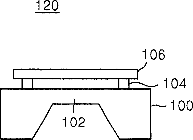
[0032] figure 2 is a cross-sectional view showing the structure of the condenser microphone.

[0033] refer to figure 2 , the gasket 104 and the vibrating plate 106 are stacked on the first side of the silicon wafer 100 , and a portion of the second side of the silicon wafer is etched to form the back plate 102 . The gasket 104 is formed by stacking an insulating film on the silicon wafer 100 and then patterning the insulating film. The vibration plate 106 is formed thereon with a conductive film. According to the illustrated structure, although the vibration plate 106 is disposed on the silicon chip 100, the positions of the vibration plate 106 and the back plate 102 can be exchanged when the vibration plate 106 and the back plate 102 are opposed to each other with the gasket 104 therebetween.

[00...


PUM


Abstract

The present invention relates to a packaging of a silicon condenser microphone and method for manufacturing the same. The packaging structure of a silicon condenser microphone of the present invention comprises a substrate having an upper surface for disposing the silicon condenser microphone and a circuit unit thereon, the substrate having a back chamber therein, the substrate including an air hole for an air to pass through between the upper surface for disposing the silicon condenser microphone and the back chamber; and a casing covering the silicon condenser microphone and the circuit unit disposed on the upper surface of the substrate for protection thereof. The method for manufacturing a packaging structure of a silicon condenser microphone of the present invention comprises steps of: (a) forming a substrate having a back chamber therein, wherein the substrate includes an air hole for an air to pass through between an upper surface of the substrate, the air hole disposed at a portion of the upper surface where the silicon condenser microphone and a circuit unit is to be disposed; (b) bonding the silicon condenser microphone and the circuit unit to the upper surface of the substrate; and (c) covering the silicon condenser microphone and the circuit unit with a casing to protect the silicon condenser microphone and the circuit unit.

Description

technical field [0001] The present invention relates to a microphone, and in particular to a packaging structure of a silicon condenser microphone and a manufacturing method thereof. Background technique [0002] In general, a microphone refers to a converter used to convert sound energy into electrical energy. A condenser microphone as one of the microphones is a microphone employing the principle of a capacitor in which two electrode plates are opposed to each other. When one of the electrode plates is used as a vibrating plate, the vibrating plate vibrates according to the sound to change the capacitance of the capacitor, thereby changing the accumulated charge. Therefore, electric current flows according to the change of sound. [0003] Among condenser microphones, an electret condenser microphone is the most well-known, and the electret condenser microphone is characterized in that an electret, which is a material including semi-permanent charges, is used instead of a...

Claims


Application Information

Patent Timeline
Patent Type & Authority Applications(China)
IPC IPC(8): H04R19/04H04R31/00
CPCH04R19/005H01L2924/10253H01L2224/48137H01L2224/48091H01L2924/00014H01L2924/00H04R19/04
Inventor 朴成镐林俊
Owner BSE CO LTD
Why Eureka
Try Eureka