Backside coating for mems wafer and its making process
一种透明基底、微机电的技术,应用在微电子微观结构装置、电路、电气元件等方向,能够解决损坏、循环时间增加、晶圆背面100b损坏等问题,达到减少负面影响、增加生产片数、减少总成本的效果
- Summary
- Abstract
- Description
- Claims
- Application Information
AI Technical Summary
Problems solved by technology
Method used
Image

Examples
Embodiment Construction
[0038]The following embodiments are to be read together with the accompanying drawings, and relative terms used in the description of the embodiments such as "lower", "higher", "horizontal", "vertical", "above", "below" , "up", "down", "top", "bottom" and their alternatives (such as "horizontally", "downward", "upward", etc.) will be described in the embodiments or shown in the drawings, These relative terms are for convenience of description and do not necessarily need to be constructed or operated in a particular orientation. Words describing figures such as "connected" or "interconnected" refer to direct contact between structures or indirect contact via intermediate structures, unless otherwise specifically described, an attachment or relationship that is both movable and rigid.
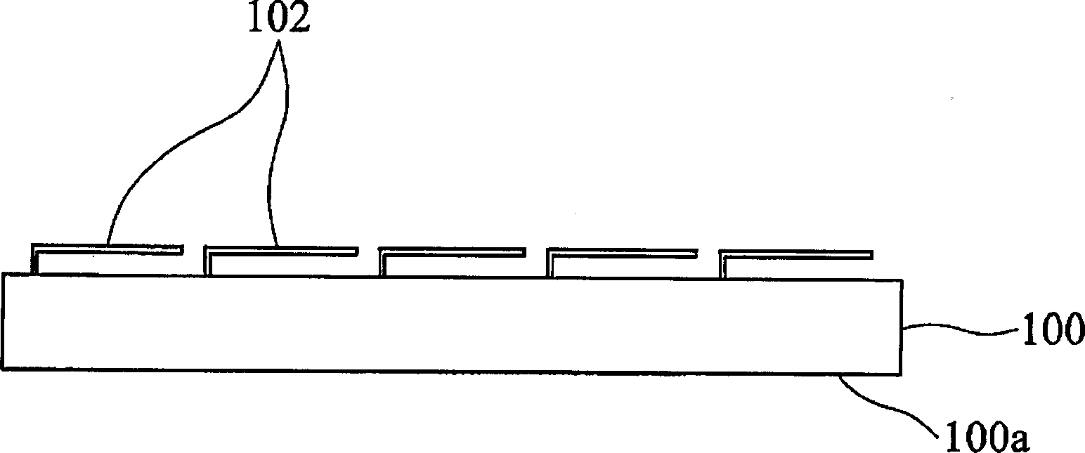
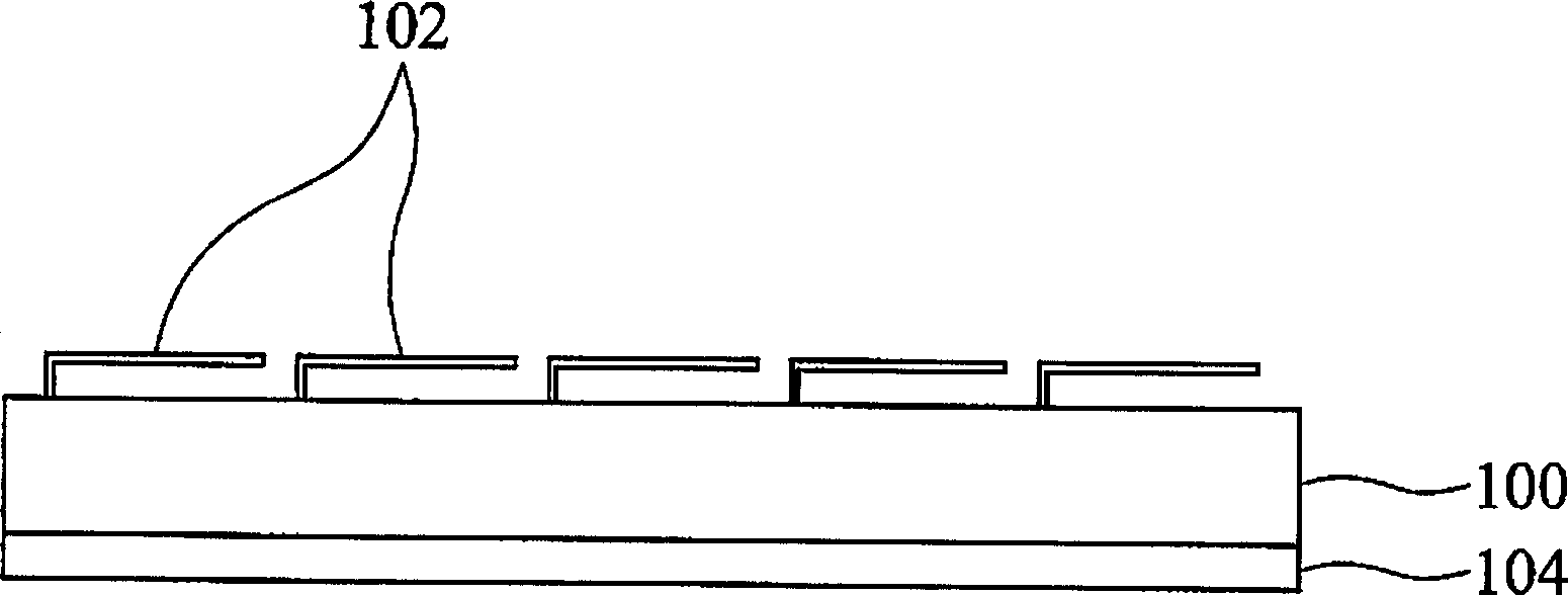
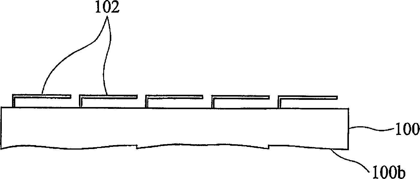
[0039] Figure 2A to Figure 2D and image 3 A method of fabricating a transparent substrate 200 having at least one microelectromechanical system (MEMS) 206 on a first side of the transparent s...
PUM
 Abstract
Description
Claims
Application Information
 - R&D
- Intellectual Property
- Life Sciences
- Materials
- Tech Scout
- Unparalleled Data Quality
- Higher Quality Content
- 60% Fewer Hallucinations
Browse by: Latest US Patents, China's latest patents, Technical Efficacy Thesaurus, Application Domain, Technology Topic, Popular Technical Reports.
© 2025 PatSnap. All rights reserved.Legal|Privacy policy|Modern Slavery Act Transparency Statement|Sitemap|About US| Contact US: help@patsnap.com